TIDT293 October   2022


  1.   Description
  2.   Features
  3.   Applications
  4. 1Design Variants
  5. 2Design Overview
    1. 2.1 Board Contents
    2. 2.2 Connector Description
    3. 2.3 User Interface
      1. 2.3.1 Switches and Push-buttons
      2. 2.3.2 Jumpers
      3. 2.3.3 Potentiometers
    4. 2.4 Functional Block Diagram
    5. 2.5 Functional Block Descriptions
  6. 3Features and Performance Curves
    1. 3.1  Test Setup
    2. 3.2  Pulse
    3. 3.3  Levels and Free Run
    4. 3.4  INP
    5. 3.5  Dual-Output Power Supply
    6. 3.6  Overtemperature Protection
    7. 3.7  Slew Rate Adjust
    8. 3.8  Settling Time Adjust
    9. 3.9  Low- and High-Level Adjust
    10. 3.10 Pulse-Width Adjust
    11. 3.11 Period and Delay Adjust
    12. 3.12 Frequency Response
  7. 4Operation
    1. 4.1 Initial Setup – Jumper Selection and Potentiometer Settings
    2. 4.2 Procedure
      1. 4.2.1 Initial Power Up
      2. 4.2.2 Connecting the Circuit Under Test
  8. 5Limitations and Capabilities
    1. 5.1 Wiring Inductance
    2. 5.2 Minimum Voltage
    3. 5.3 Battery Life
  9. 6Typical Failure Mechanism
    1. 6.1 Fast Thermal Failure
    2. 6.2 Slow Thermal Failure

Fast Thermal Failure

Fast thermal failure occurs usually in high-voltage operation when the SOA rating of the MOSFET is exceeded. Generally, the FET (Q2) shorts, the sense resistor (R21) opens, the gate resistor (R14) is damaged, and the THS3120 op amp (U4) fails.

The following waveform shows a capture of a full-range step after damage to the load switch driver U4.
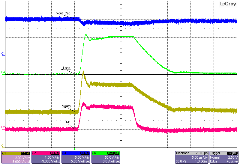
GUID-20220531-SS0I-0C7S-QJPH-TF9KPFH6ZKB1-low.png Figure 6-1 1-A to 100-A Step, 10-V Output, Maximum Slew Rate, Damaged U4

The following image shows the same response after replacing U4.

GUID-20220531-SS0I-T8QD-X2LV-ZMSW14QCZ0WH-low.png Figure 6-2 1-A to 100-A Step, 10-V Output, Maximum Slew Rate, Replaced U4