TIDT293 October 2022
3.1 Test Setup
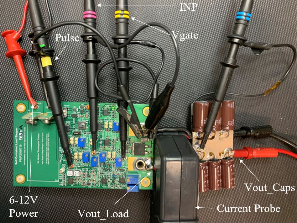
Figure 3-1 shows the setup used to test each function of the board. A Chroma 62000P bench supply is used along with a capacitor bank consisting of six 470-μF aluminum capacitors to holdup the voltage. The capacitor bank is used to emulate a device under test (DUT). The capacitors represent the output filter of a typical power supply being tested.
The current probe used is the CP150 to avoid probe saturation for large load steps. Minimize the wiring inductive loop between the load step board and test device if high a slew rate (100 A/μs) is desired.
 Figure 3-1 Setup for Testing the Load Step Board Using a Power Supply
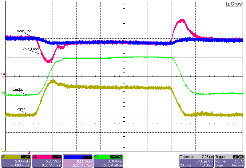
Vout_Load is the drain-source voltage of Q2 which droops as the gate voltage increases and drain-source current rises. Minimize this voltage droop to keep Q2 out of saturation (see the limitations of wiring inductance and minimum voltage).
Measuring at the capacitor bank represents the response of the bench supply to the load step. The capture in Figure 3-2 shows the difference between the two output voltage measurements.
 Figure 3-2 The Difference in Measuring Both Sides of the Capacitor Bank When Testing With the Chroma 62000p
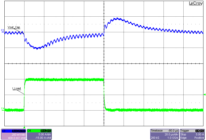
When testing a converter, the Vout_Cap waveform depends on the control loop characteristics such as crossover frequency and phase margin. The load step requires a fast transition with respect to the converter bandwidth to fully exercise the control loop of the DUT.
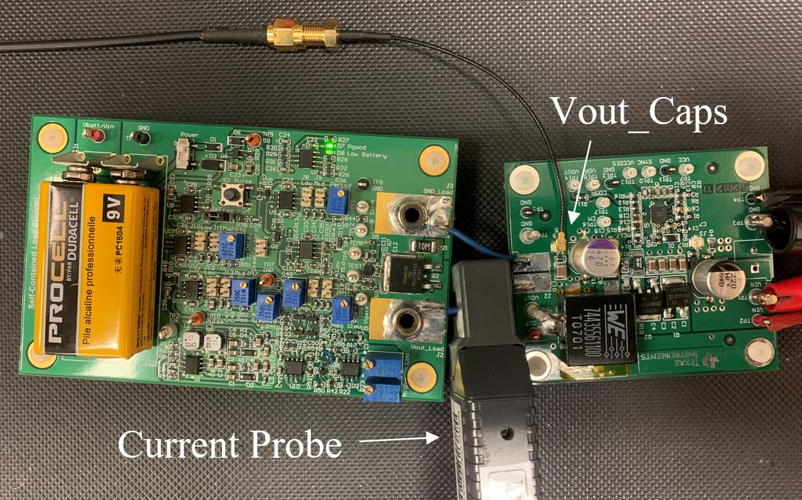
Figure 3-3 shows the setup to test a converter using the PMP20967 load step board. A synchronous buck 12-V output reference design was used in this example. The output voltage response to the load step exhibits characteristics of a stable loop with a 15-kHz crossover frequency.
For best measurement accuracy of the output voltage response, a single voltage probe with ground at the DUT is used. A PCB coax probe connector with 50-Ω termination is used for this example.
 Figure 3-3 Setup for Using the Load Step Board With a Converter Under Test
 Figure 3-4 Load Transient Test on 12-V Output Synchronous Buck