TIDUDT4A May 2018 – November 2021 AM3351 , AM3352 , AM3354 , AM3356 , AM3357 , AM3358 , AM3358-EP , AM3359
- Description
- Resources
- Features
- Applications
- 5
- 1System Description
- 2System Overview
- 3Hardware, Software, Testing Requirements, and Test Results
- 4Design Files
- 5Software Files
- 6Related Documentation
- 7About the Author
- 8Revision History
3.1.1.1 Connector Configuration of TIDA-01568
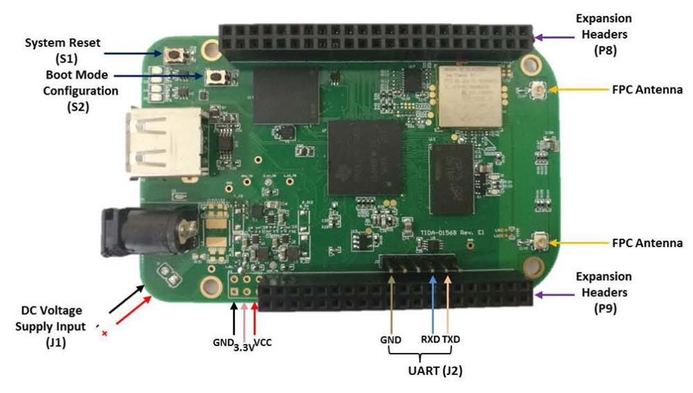
Figure 3-1 shows the top view of the PCB and connector configuration for this reference design, that features the following:
- A two-terminal input for power supply (J1): This pin is used to connect the input DC supply. The positive and negative terminals are also shown in Figure 3-1.
- A six-pin connector for UART (J2): Three of the pins are used for external UART communication with a host machine. This interface is usually used for monitoring booting information during Linux software development.
- System Reset (S1): This switch is used to reset the processors.
- Boot Mode Configuration (S2): This switch is used to change boot mode between two modes. The usual operation is to change boot from the on-board flash to an external microSD card.
- Expansion headers (P8,P9): These two headers lead out the processors' available GPIOs and on-chip resources, which can be used for expand functions, including 67 GPIOs, 4 timers, 4 UARTs, 8 PWMs, 1 24-bit LCD controller, 1 MMC, 7 ADCs, 2 I2Cs, and 2 SPIs.
- PFC Antenna: These two terminals are used for installing 2.4G / 5G PFC antennas in UFL/IPEX-1 type.
 Figure 3-1 PCB Top View and Connector
Configuration
Figure 3-1 PCB Top View and Connector
ConfigurationTable 3-1 and Table 3-2 shows the pin layout and corresponding pin connection and functions.
Table 3-1 Expansion Headers – P8
| CORRESPONDING CONNECTION | PIN NUMBER | PIN NUMBER | CORRESPONDING CONNECTION |
|---|---|---|---|
| DGND | 1 | 2 | DGND |
| GPIO1_6 | 3 | 4 | GPIO1_7 |
| GPIO1_2 | 5 | 6 | GPIO1_3 |
| GPIO2_2 TIMER4 | 7 | 8 | GPIO2_3 TIMER7 |
| GPIO2_5 TIMER5 | 9 | 10 | GPIO2_4 TIMER6 |
| GPIO1_13 LCD_DATA18 | 11 | 12 | GPIO1_12 LCD_DATA19 |
| GPIO0_23 EHRPWM2B LCD_DATA22 | 13 | 14 | GPIO0_26 LCD_DATA21 |
| GPIO1_15 LCD_DATA16 | 15 | 16 | GPIO1_14 LCD_DATA17 |
| GPIO0_27 LCD_DATA20 | 17 | 18 | GPIO2_1 |
| GPIO0_22 EHRPWM2A LCD_DATA23 | 19 | 20 | GPIO1_31 MMC1_CMD |
| GPIO1_30 MMC1_CLK | 21 | 22 | GPIO1_5 MMC1_DAT5 |
| GPIO1_4 MMC1_DAT4 | 23 | 24 | GPIO1_1 MMC1_DAT1 |
| GPIO1_0 MMC1_DAT0 | 25 | 26 | GPIO1_29 |
| GPIO2_22 LCD_VSYNC | 27 | 28 | GPIO2_24 LCD_PCLK |
| GPIO2_23 LCD_HSYNC | 29 | 30 | GPIO2_25 LCD_DE |
| GPIO0_10 LCD_DATA14 UART5_CTSN+ | 31 | 32 | GPIO0_11 LCD_DATA15 UART5_RTSN |
| GPIO0_9 LCD_DATA13 UART4_RTSN | 33 | 34 | GPIO2_17 LCD_DATA11 EHRPWM1B UART3_RTSN |
| GPIO0_8 LCD_DATA12 UART4_CTSN | 35 | 36 | GPIO2_16 LCD_DATA10 EHRPWM1A UART3_CTSN |
| GPIO2_14 LCD_DATA8 UART5_TXD+ | 37 | 38 | GPIO2_13 LCD_DATA9 UART5_RXD+ |
| GPIO2_12 LCD_DATA6 | 39 | 40 | GPIO2_11 LCD_DATA7 |
| GPIO2_10 LCD_DATA4 | 41 | 42 | GPIO2_9 LCD_DATA5 |
| GPIO2_8 LCD_DATA2 | 43 | 44 | GPIO2_7 LCD_DATA3 |
| GPIO2_6 LCD_DATA0 EHRPWM2A | 45 | 46 | GPIO2_5 LCD_DATA1 EHRPWM2B |
Table 3-2 Expansion Headers – P9
| CORRESPONDING CONNECTION | PIN NUMBER | PIN NUMBER | CORRESPONDING CONNECTION |
|---|---|---|---|
| DGND | 1 | 2 | DGND |
| 3.3 V | 3 | 4 | 3.3 V |
| 5.0 V | 5 | 6 | 5.0 V |
| 5.0 V | 7 | 8 | 5.0 V |
| EXTINTn | 9 | 10 | SYS_RESETn |
| GPIO0_30 UART4_RXD | 11 | 12 | GPIO1_28 |
| GPIO0_31 UART4_TXD | 13 | 14 | GPIO1_18 EHRPWM1A |
| GPIO1_16 | 15 | 16 | GPIO1_19 EHRPWM1B |
| GPIO0_5 I2C1_SCL SPI1_CS0 | 17 | 18 | GPIO0_4 I2C1_SDA SPI1_D1 |
| GPIO0_13 I2C2_SCL UART1_RTSn SPI1_CS1 | 19 | 20 | GPIO0_12 I2C2_SDA UART1_CTSn SPI1_CS0 |
| I2C2_SCL SPI0_D0 GPIO0_3 UART2_TXD EHRPWM0B | 21 | 22 | SPI0_SCLK GPIO0_2 UART2_RXD EHRPWM0A I2C2_SDA |
| GPIO1_17 | 23 | 24 | GPIO0_15 UART1_TXD I2C1_SCL |
| GPIO3_21 | 25 | 26 | GPIO0_14 UART1_RXD I2C2_SDA |
| GPIO3_19 | 27 | 28 | GPIO3_17 SPI1_CS0 ECAPPWM2 |
| GPIO3_15 SPI1_D0 EHRPWM0B | 29 | 30 | GPIO3_16 SPI1_D1 |
| GPIO3_14 SPI1_SCLK EHRPWM0A | 31 | 32 | VDD_ADC |
| AIN6 | 33 | 34 | GNDA_ADC |
| AIN4 | 35 | 36 | AIN5 |
| AIN2 | 37 | 38 | AIN3 |
| AIN0 | 39 | 40 | AIN1 |
| GPIO0_20 | 41 | 42 | GPIO0_7 ECAPPWM0 SPI1_CS1 |
| DGND | 43 | 44 | DGND |
| DGND | 45 | 46 | DGND |