TIDUEM8B March 2019 – February 2021
2.1 Block Diagram
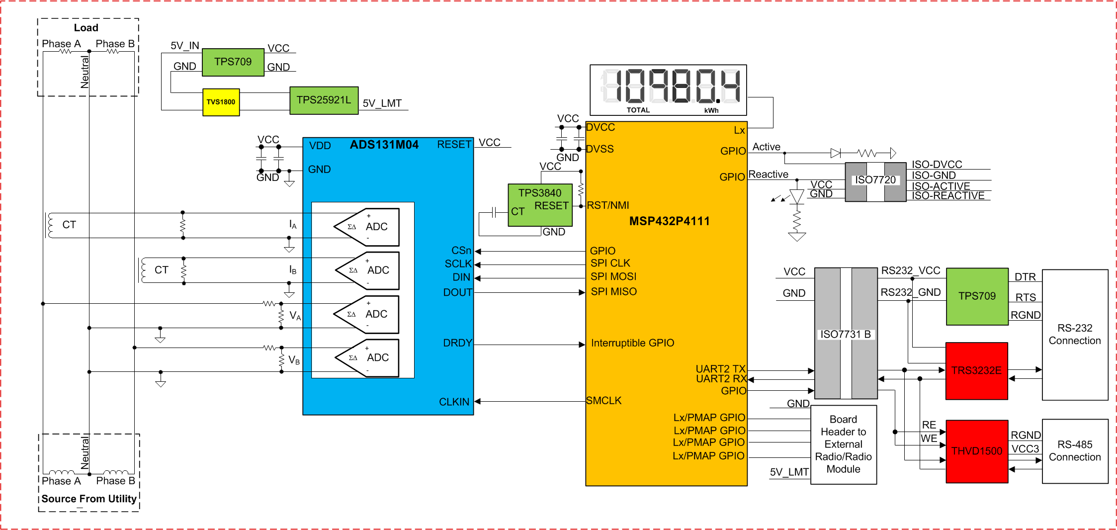
Figure 2-1 and Figure 2-2 depict block diagrams that show the high-level interface used for an ADS131M04-based split-phase energy measurement application. For the two-voltage configuration, the line-to-neutral voltage is directly measured for each line wire. For the one-voltage configuration, in comparison, only the line-to-line voltage is directly measured instead of the line-to-neutral voltages.
 Figure 2-1 TIDA-010037 Block Diagram, Two-Voltage Configuration
 Figure 2-2 TIDA-010037 Block Diagram, One-Voltage Configuration
In the diagrams, a current sensor connects to the current channels and a simple voltage divider is used for the corresponding voltage. The CT has an associated burden resistor that must be connected at all times to protect the measuring device. The selection of the CT and the burden resistor is made based on the manufacturer and current range required for energy measurements.
The choice of voltage divider resistors for the voltage channel is selected to ensure the mains voltage is divided down to adhere to the normal input ranges of the ADS131M04 device. Since the ADS131M04 ADCs have a large dynamic range and a large dynamic range is not needed to measure voltage, the voltage front-end circuitry is purposely selected so that the maximum voltage seen at the inputs of the voltage channel ADCs are only a fraction of the full-scale voltage. By reducing the voltage fed to the ADS131M04 voltage ADC, voltage to current crosstalk, which actually affects metrology accuracy more than voltage ADC accuracy, is reduced at the cost of voltage accuracy, thereby resulting in more accurate energy measurements at lower currents.
In this design, the ADS131M04 device interacts with the MSP432™ MCU in the following manner:
- The CLKIN clock used by the ADS131M04 device is provided from the SMCLK clock signal output of the MSP432 MCU.
- The ADS131M04 device divides the clock provided on its CLKIN pin by two and uses this divided clock as its delta-sigma modulation clock.
- When new ADC samples are ready, the ADS131M04 device asserts its DRDY pin, which alerts the MSP432 MCU that new samples are available.
- After being alerted of new samples, the MSP432 MCU uses one of its SPI interfaces and its DMA to get the voltage and current samples from the ADS131M04 device.
In this design, a TPS3840 device is used as an external SVS for the MSP432 MCU. Although the MSP432 MCU has an internal SVS that suffices for this application, the TPS3840 standalone SVS is used because there is additional security in having a SVS that is independent of the MCU.
Other signals of interest in Figure 2-1 and Figure 2-2 are the active and reactive energy pulses used for accuracy measurement and calibration. The ISO7720 device provides an isolated connection for these pulses for connecting to non-isolated equipment. This is especially needed for the one-voltage configuration since the system is referenced with respect to one of the two high-voltage line voltages for this configuration.
In addition to isolated pulses, the design supports isolated RS-232 communication through the use of the TPS70933, ISO7731B, and TRS3232E devices. The design can be configured to use RS-485 as well instead of RS-232 through the use of the ISO7731B and THVD1500 devices on the board.
The design also supports communication using external radios or radio modules that are connected to the J11 and J12 headers of the board. The J11 header connects the P7.0, P7.1, P7.2, and P7.3 port pins, which can be configured as port mappable GPIO pins, if the LCD is disabled. Software can be added to the MSP432 MCU to communicate to an external radio or radio module by configuring any of these four pins as communication pins(SPI or UART) and appropriately writing and reading packets to and from them. The J12 header is the power rail and GND connection to the radio. The power rail on J12 is the current-limited version of the 5V_IN rail at J4. The J12 power rail is specifically current limited to 1.6 A by the TPS25921L device. If there is a short on the radio module or the current exceeds 1.6 A for some reason, the power to this rail will be limited to prevent the power supply from affecting the power to the metrology-relevant portions of this board. If it is a transient overcurrent event, the module continues to receive power and operate without interruption. However, if there is a persistent fault on the module, the TPS25921L device will enter thermal shutdown and power is disconnected. After this thermal shutdown event, the power can only be reconnected to the radio module manually by driving the P5.2 GPIO pin. In addition, if the voltage fed to the 5V_IN rail at J4 is below approximately 4.0 V or above 5.8 V, the TPS25921L device is configured to disconnect the power rail on J12. To protect the TPS25921L device from any transients due to switching, a TVS1800 transient protection device is connected to this device.
The design can be powered either by applying 3.3 V at the DVCC header(J9) directly or through the TPS70933 device by applying 5 V at the 5V_IN header(J4). See Table 3-1 for more details on the proper jumper connections for powering the board for both options.