TIDUEM8B March 2019 – February 2021
2.3.1.4.1 Voltage Measurement Analog Front End
The nominal voltage from the mains is from 100 V–240 V so it needs to be scaled down to be sensed by an ADC. Figure 2-5 shows the analog front end used for this voltage scaling. J28 is where the voltage is applied.
 Figure 2-5 Analog Front End for Voltage Inputs
In the analog front end for voltage, there consists a spike protection varistor (R87), footprints for electromagnetic interference filter beads (resistor footprints R103 and R104) , a voltage divider network (R105, R106, R107, and R108), and an RC low-pass filter (R109, R110, C103, C104, and C105).
At lower currents, voltage-to-current crosstalk affects active energy accuracy much more than voltage accuracy, if power offset calibration is not performed. To maximize the accuracy at these lower currents, in this design the entire ADC range is not used for voltage channels. Since the ADCs of the ADS131M04 device are high-accuracy ADCs, using the reduced ADC range for the voltage channels in this design still provides more than enough accuracy for measuring voltage. Equation 1 shows how to calculate the range of differential voltages fed to the voltage ADC channel for a given Mains voltage and selected voltage divider resistor values.
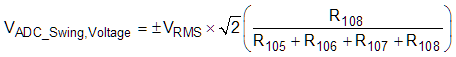
Based on this formula and the selected resistor values in Figure 2-5, for a mains voltage of 120 V (as measured between the line and neutral), the input signal to the voltage ADC has a voltage swing of ±128 mV (91 mVRMS) when using the two-voltage configuration. For the one-voltage configuration, for a mains voltage of 120 V (as measured between the line and neutral), 240 V would be input to the front-end circuit in Figure 2-5 since the line-to-line voltage is measured instead of the line-to-neutral voltage. The 240-V input to the front-end circuit produces a voltage swing of ±257 mV (182 mVRMS). The ±128-mV and the ±257-mV voltage ranges for the two-voltage and one-voltage configurations are both well within the ±1.2-V input voltage that can be sensed by the ADS131M04 device for the selected PGA gain value of 1 that is used for the voltage channels.
Note that the pin order of the AINxP and AINxN pins on the ADS131M04 is swapped when going from one converter to another. As an example, AIN2P is pin 7 and AIN2N is pin 8 but AIN3N is pin 9 and AIN3P is pin 10. The swapped order is why the order of the positive input voltage and negative input voltage is swapped between the J28 voltage input terminal block of Phase A and the J29 voltage input terminal block of Phase B.