TIDUEO0C July 2019 – March 2021
- Description
- Resources
- Features
- Applications
- 5
- 1System Description
-
2System Overview
- 2.1 Block Diagram
- 2.2 Design Considerations
- 2.3
Highlighted Products
- 2.3.1 TPS63900: 1.8V-5.5 VIN Buck-Boost Converter With 75-nA Ultra-low Quiescent Current and 400-mA Output Current
- 2.3.2 TPS610995: 0.7 VIN Synchronous Boost Converter With 400-nA Ultra-low Quiescent Current and 1-A Peak Current
- 2.3.3 TPS62840: 750-mA Synchronous Step-Down Converter With Ultra-low Quiescent Current Consumption
- 2.4 System Design Theory
- 3Hardware, Software, Testing Requirements, and Test Results
- 4Design Files
- 5Software Files
- 6Related Documentation
- 7Terminology
- 8About the Author
- 9Revision History
2.3.3 TPS62840: 750-mA Synchronous Step-Down Converter With Ultra-low Quiescent Current Consumption
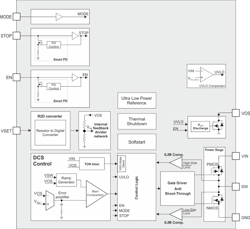
The TPS62840 device is a synchronous step-down converter with ultra-low quiescent current consumption. Using TI's DCS-Control™ topology the device extends the high efficiency operation area down to micro amperes of load current during Power-Save Mode Operation.
TI's DCS-Control (Direct Control with Seamless Transition into Power-Save Mode) is an advanced regulation topology, which combines the advantages of hysteretic and voltage mode controls. Characteristics of DCSControl include excellent AC load regulation and transient response, low output ripple voltage, and a seamless transition between PFM and PWM mode operation. DCS-Control includes an AC loop which senses the output voltage (VOS pin) and directly feeds this information into a fast comparator stage.
The device operates with a quasi-fixed frequency of 1.8 MHz (typ). A high gain voltage feedback loop is used to achieve accurate DC load regulation. To save extra quiescent current under light-load condition ( that is, IOUT in the mA range), the internal error amplifier is powered down with a minimum influence on the DC line and load regulation characteristic. The internally compensated regulation network achieves fast and stable operation with small external components and low ESR capacitors.
In Power-Save Mode, the switching frequency varies linearly with the load current. Since DCS-Control supports both operating modes with one single building block, the transition from PWM to PFM is seamless with minimum output voltage ripple. The TPS62840 device offers both excellent DC voltage and superior load transient regulation, combined with low-output voltage ripple thereby minimizing interferences with RF circuits.
 Figure 2-4 TPS62840 Functional Block Diagram
At light load conditions it seamlessly enters power save mode to reduce switching cycles and maintain high efficiency. There are 16 predefined output voltages that can be selected by connecting a resistor to the VSEL pin making the device flexible for various applications with a minimum amount of external components.