TIDUEO0C July 2019 – March 2021
- Description
- Resources
- Features
- Applications
- 5
- 1System Description
-
2System Overview
- 2.1 Block Diagram
- 2.2 Design Considerations
- 2.3
Highlighted Products
- 2.3.1 TPS63900: 1.8V-5.5 VIN Buck-Boost Converter With 75-nA Ultra-low Quiescent Current and 400-mA Output Current
- 2.3.2 TPS610995: 0.7 VIN Synchronous Boost Converter With 400-nA Ultra-low Quiescent Current and 1-A Peak Current
- 2.3.3 TPS62840: 750-mA Synchronous Step-Down Converter With Ultra-low Quiescent Current Consumption
- 2.4 System Design Theory
- 3Hardware, Software, Testing Requirements, and Test Results
- 4Design Files
- 5Software Files
- 6Related Documentation
- 7Terminology
- 8About the Author
- 9Revision History
2.3.2 TPS610995: 0.7 VIN Synchronous Boost Converter With 400-nA Ultra-low Quiescent Current and 1-A Peak Current
The TPS610995 device is a synchronous boost converter with 1-µA max and 400nA typical ultra-low quiescent current. The device is designed for products powered by an alkaline battery, nickel metal hydride (NiMH) rechargeable battery, LiMnO2 battery or rechargeable lithium-ion (Li-Ion) battery, for which high efficiency under light load conditions is critical to achieve long battery life.
The TPS610995 boost converter uses a hysteretic control topology to obtain maximal efficiency at minimal quiescent current. It only consumes 1-µA quiescent current under light load conditions and can achieve up to 75% efficiency at 10-µA load with fixed output voltage version. It can also support up to 300-mA output current from 3.3-V to 5-V conversion, and achieve up to 93% at 200-mA load.
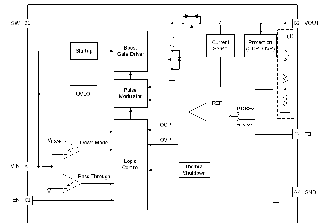
 Figure 2-3 TPS610995 Functional Block Diagram
The TPS610995 also offers both down mode and pass-through operations for different applications. In down mode, the output voltage can still be regulated at target value even when the input voltage is higher than output voltage. In pass-through mode, the output voltage follows the input voltage. The TPS610995 exits down mode and enters into pass-through mode when VIN > VOUT + 0.5 V.
The TPS61099 family of devices supports true shutdown function when it is disabled, which disconnects the load from the input supply to reduce the current consumption. There are both adjustable output voltage version and fixed output voltage device versions, such as the TPS610995 device which is used in this reference design. It is available in 6-ball, 1.23-mm × 0.88-mm WCSP package and 6-pin 2-mm ×
2-mm WSON package.