TIDUEO0C July 2019 – March 2021
- Description
- Resources
- Features
- Applications
- 5
- 1System Description
-
2System Overview
- 2.1 Block Diagram
- 2.2 Design Considerations
- 2.3
Highlighted Products
- 2.3.1 TPS63900: 1.8V-5.5 VIN Buck-Boost Converter With 75-nA Ultra-low Quiescent Current and 400-mA Output Current
- 2.3.2 TPS610995: 0.7 VIN Synchronous Boost Converter With 400-nA Ultra-low Quiescent Current and 1-A Peak Current
- 2.3.3 TPS62840: 750-mA Synchronous Step-Down Converter With Ultra-low Quiescent Current Consumption
- 2.4 System Design Theory
- 3Hardware, Software, Testing Requirements, and Test Results
- 4Design Files
- 5Software Files
- 6Related Documentation
- 7Terminology
- 8About the Author
- 9Revision History
3.2.2.2 Test Results With the TPS610995 Boost Converter

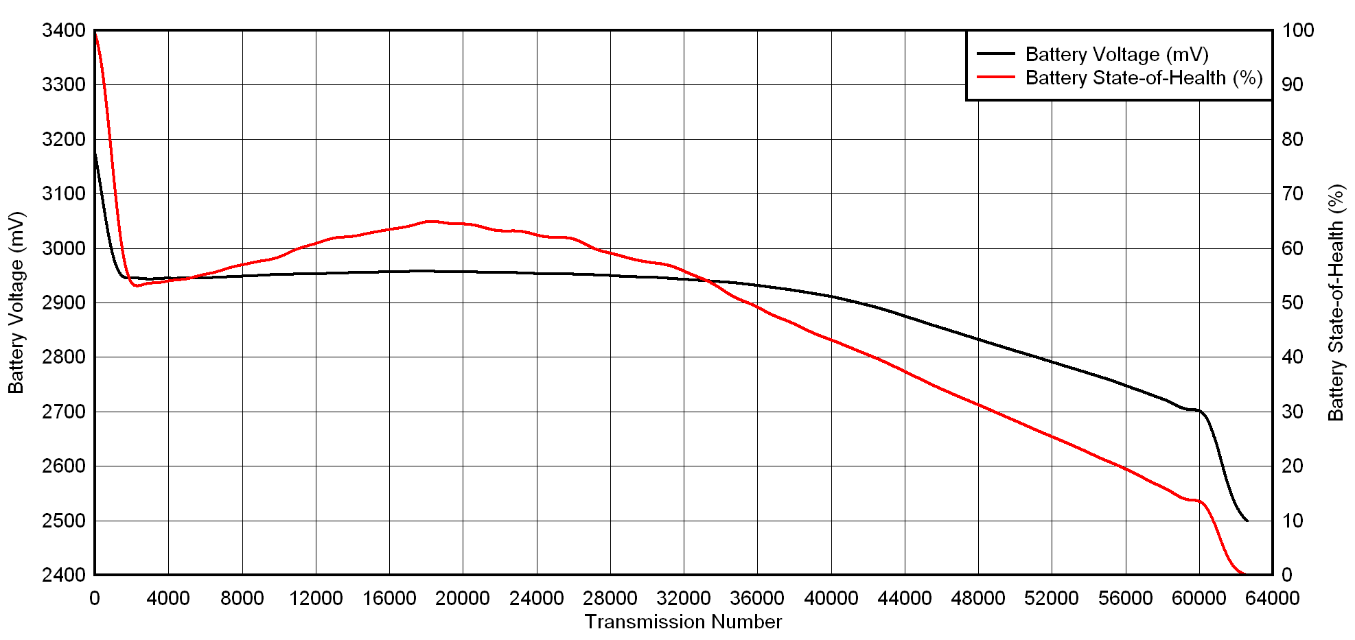
Figure 3-10 highlights how using this power solution for an NB-IoT module, 61,000 transmissions (taken at 10% SOH) can be supported. Similarly to the buck converter discharge data, stand-by current will play an added role in a field application, in addition to the 250-mA pulses. Refer to Section 3.2.2.4 for analysis on battery lifetime estimations for this topology.
As detailed in Section 3.2.2.1, the BQ35100 device will perform best once the cell voltage starts decreasing more meaningfully. This can be observed around the midpoint at 35,000 transmissions where SOH equates to 50%, then the SOH reading becomes roughly linear and hones in on 0% SOH. See the FDK Lithium CR17500EP LiMnO2 Primary Battery Data Sheet to observe typical voltage discharge curves.
In this test, the TPS610995 device operates at VOUT = 3.6 V to power the NB-IoT modules. With a smaller voltage level difference between VIN and VOUT, it will deliver several percent points higher efficiency numbers than those in the data sheet plot.