SCPS145B December 2007 – February 2016 P82B715
PRODUCTION DATA.
- 1 Features
- 2 Applications
- 3 Description
- 4 Revision History
- 5 Pin Configuration and Functions
- 6 Specifications
- 7 Parameter Measurement Information
- 8 Detailed Description
- 9 Application and Implementation
- 10Power Supply Recommendations
- 11Layout
- 12Device and Documentation Support
- 13Mechanical, Packaging, and Orderable Information
パッケージ・オプション
メカニカル・データ(パッケージ|ピン)
サーマルパッド・メカニカル・データ
発注情報
1 Features
- Operating Power-Supply Voltage Range of 3 V to 12 V
- Supports Bidirectional Data Transfer of I2C Bus Signals
- Allows Bus Capacitance of 400 pF on Main I2C Bus (Sx/Sy Side) and 3000 pF on Transmission Side (Lx/Ly Side)
- Dual Bidirectional Unity-Voltage-Gain Buffer With No External Directional Control Required
- Drives 10× Lower-Impedance Bus Wiring for Improved Noise Immunity
- Multi-Drop Distribution of I2C Signals Using Low-Cost Twisted-Pair Cables
- I2C Bus Operation Over 50 Meters of Twisted-Pair Wire
- Latch-up Performance Exceeds 100 mA Per JESD 78, Class II
- ESD Protection Exceeds JESD 22
2 Applications
- HDMI DDC
- Long I2C Communications
- Industrial Communications
3 Description
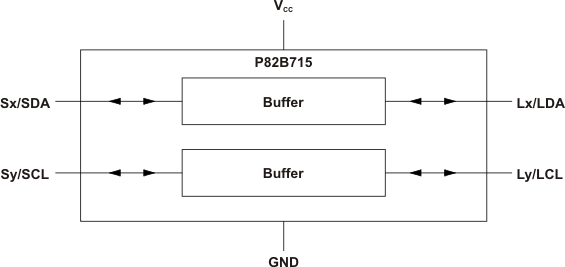
The P82B715 is a device for buffering highly-capacitive I2C bus systems, and it supports bidirectional data transfer through the I2C bus. The P82B715 buffers both the serial data (SDA) and serial clock (SCL) signals on the I2C bus and allows for extension of the I2C bus, while retaining all the operating modes and features of the I2C system.
Device Information(1)
| PART NUMBER | PACKAGE | BODY SIZE (NOM) |
|---|---|---|
| P82B715 | SOIC (8) | 4.90 mm × 3.91 mm |
| PDIP (8) | 9.81 mm × 6.35 mm |
- For all available packages, see the orderable addendum at the end of the data sheet.
Block Diagram
