SBAS582C July 2014 – April 2015 ADS8684 , ADS8688
PRODUCTION DATA.
- 1 Features
- 2 Applications
- 3 Description
- 4 Revision History
- 5 Device Comparison Table
- 6 Pin Configuration and Functions
- 7 Specifications
-
8 Detailed Description
- 8.1 Overview
- 8.2 Functional Block Diagram
- 8.3 Feature Description
- 8.4
Device Functional Modes
- 8.4.1 Device Interface
- 8.4.2
Device Modes
- 8.4.2.1 Continued Operation in the Selected Mode (NO_OP)
- 8.4.2.2 Frame Abort Condition (FRAME_ABORT)
- 8.4.2.3 STANDBY Mode (STDBY)
- 8.4.2.4 Power-Down Mode (PWR_DN)
- 8.4.2.5 Auto Channel Enable with Reset (AUTO_RST)
- 8.4.2.6 Manual Channel n Select (MAN_Ch_n)
- 8.4.2.7 Channel Sequencing Modes
- 8.4.2.8 Reset Program Registers (RST)
- 8.5
Register Maps
- 8.5.1 Command Register Description
- 8.5.2
Program Register Description
- 8.5.2.1 Program Register Read/Write Operation
- 8.5.2.2 Program Register Map
- 8.5.2.3 Program Register Descriptions
- 9 Application and Implementation
- 10Power-Supply Recommendations
- 11Layout
- 12Device and Documentation Support
- 13Mechanical, Packaging, and Orderable Information
1 Features
- 16-Bit ADCs with Integrated Analog Front-End
- 4-, 8-Channel MUX with Auto and Manual Scan
- Channel-Independent Programmable Input Ranges:
- 5-V Analog Supply: 1.65-V to 5-V I/O Supply
- Constant Resistive Input Impedance: 1 MΩ
- Input Overvoltage Protection: Up to ±20 V
- On-Chip, 4.096-V Reference with Low Drift
- Excellent Performance:
- 500-kSPS Aggregate Throughput
- DNL: ±0.5 LSB; INL: ±0.75 LSB
- Low Drift for Gain Error and Offset
- SNR: 92 dB; THD: –102 dB
- Low Power: 65 mW
- AUX Input → Direct Connection to ADC Inputs
- SPI™-Compatible Interface with Daisy-Chain
- Industrial Temperature Range: –40°C to 125°C
- TSSOP-38 Package (9.7 mm × 4.4 mm)
2 Applications
- Power Automation
- Protection Relays
- PLC Analog Input Modules
3 Description
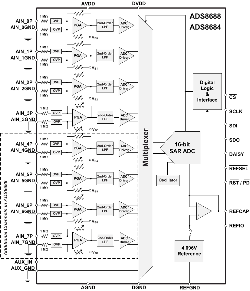
The ADS8684 and ADS8688 are 4- and 8-channel, integrated data acquisition systems based on a 16-bit successive approximation (SAR) analog-to-digital converter (ADC), operating at a throughput of
500-kSPS. The devices feature integrated analog front-end circuitry for each input channel with overvoltage protection up to ±20 V, a 4- or 8-channel multiplexer with automatic and manual scanning modes, and an on-chip, 4.096-V reference with low temperature drift. Operating on a single 5-V analog supply, each input channel on the devices can support true bipolar input ranges of ±10.24 V,
±5.12 V, and ±2.56 V, as well as unipolar input ranges of 0 V to 10.24 V and 0 V to 5.12 V. The gain of the analog front-end for all input ranges is accurately trimmed to ensure a high dc precision. The input range selection is software-programmable and independent for each channel. The devices offer a
1-MΩ constant resistive input impedance irrespective of the selected input range.
The ADS8684 and ADS8688 offer a simple SPI-compatible serial interface to the digital host and also support daisy-chaining of multiple devices. The digital supply operates from 1.65 V to 5.25 V, enabling direct interface to a wide range of host controllers.
Device Information(1)
| PART NUMBER | PACKAGE | BODY SIZE (NOM) |
|---|---|---|
| ADS868x | TSSOP (38) | 9.70 mm × 4.40 mm |
- For all available packages, see the orderable addendum at the end of the datasheet.
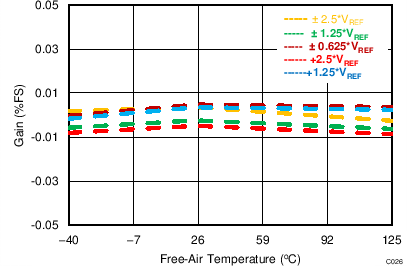
Gain Error versus Temperature

4 Revision History
Changes from B Revision (August 2014) to C Revision
- Changed unipolar sub-bullet of third Features bulletGo
- Added title to page 1 block diagram Go
- Deleted footnote from Device Comparison table Go
- Updated ESD Ratings table to current standards Go
- Corrected package name in Thermal Information table Go
- Changed Auxiliary Channel, SINAD and SFDR typical specifications in Electrical Characteristics table Go
- Changed tDZ_CSDO symbol in Timing Requirements table and Figure 1Go
- Deleted clamp from second sentence of Overview section Go
- Changed voltage range values in second paragraph of Analog Inputs section Go
- Changed Range_CHn[2:0] to Range_CHn[3:0] in Programmable Gain Amplifier (PGA) sectionGo
- Added Bit 3 column to Table 3Go
- Changed SDO to SDI in second sentence of Event 3 in Data Acquisition Example section Go
- Changed Continued Operation in the Selected Mode sectionGo
- Changed Frame Abort Condition sectionGo
- Changed STANDBY Mode section: added clarification to description of STANDBY modeGo
- Changed second paragraph of Power-Down Mode section: added clarification to description of PWR_DN mode Go
- Changed first two paragraphs of Auto Channel Enable with Reset sectionGo
- Changed first paragraph of Manual Channel n Select section Go
- Changed second paragraph of Reset Program Registers section: added clarity to description of RST mode Go
- Changed Program Register Description section Go
Changes from A Revision (July 2014) to B Revision
- Made changes to product preview data sheet, released to Production DataGo
Changes from * Revision (July 2014) to A Revision
- Made changes to product preview data sheetGo
