SWRS177B February 2015 – July 2016 CC2630
PRODUCTION DATA.
- 1Device Overview
- 2Revision History
- 3 Device Comparison
- 4Terminal Configuration and Functions
-
5Specifications
- 5.1 Absolute Maximum Ratings
- 5.2 ESD Ratings
- 5.3 Recommended Operating Conditions
- 5.4 Power Consumption Summary
- 5.5 General Characteristics
- 5.6 IEEE 802.15.4 (Offset Q-PSK DSSS, 250 kbps) - RX
- 5.7 IEEE 802.15.4 (Offset Q-PSK DSSS, 250 kbps) - TX
- 5.8 24-MHz Crystal Oscillator (XOSC_HF)
- 5.9 32.768-kHz Crystal Oscillator (XOSC_LF)
- 5.10 48-MHz RC Oscillator (RCOSC_HF)
- 5.11 32-kHz RC Oscillator (RCOSC_LF)
- 5.12 ADC Characteristics
- 5.13 Temperature Sensor
- 5.14 Battery Monitor
- 5.15 Continuous Time Comparator
- 5.16 Low-Power Clocked Comparator
- 5.17 Programmable Current Source
- 5.18 Synchronous Serial Interface (SSI)
- 5.19 DC Characteristics
- 5.20 Thermal Resistance Characteristics
- 5.21 Timing Requirements
- 5.22 Switching Characteristics
- 5.23 Typical Characteristics
- 6Detailed Description
- 7Application, Implementation, and Layout
- 8Device and Documentation Support
- 9Mechanical Packaging and Orderable Information
パッケージ・オプション
デバイスごとのパッケージ図は、PDF版データシートをご参照ください。
メカニカル・データ(パッケージ|ピン)
- RSM|32
- RHB|32
- RGZ|48
サーマルパッド・メカニカル・データ
発注情報
1 Device Overview
1.1 Features
- Microcontroller
- Powerful ARM® Cortex®-M3
- EEMBC CoreMark® Score: 142
- Up to 48-MHz Clock Speed
- 128KB of In-System Programmable Flash
- 8KB of SRAM for Cache
- 20KB of Ultralow-Leakage SRAM
- 2-Pin cJTAG and JTAG Debugging
- Supports Over-The-Air Upgrade (OTA)
- Ultralow-Power Sensor Controller
- Can Run Autonomous From the Rest of the System
- 16-Bit Architecture
- 2KB of Ultralow-Leakage SRAM for Code and Data
- Efficient Code Size Architecture, Placing Drivers, IEEE 802.15.4 MAC, and Bootloader in ROM
- RoHS-Compliant Packages
- 4-mm × 4-mm RSM VQFN32 (10 GPIOs)
- 5-mm × 5-mm RHB VQFN32 (15 GPIOs)
- 7-mm × 7-mm RGZ VQFN48 (31 GPIOs)
- Peripherals
- All Digital Peripheral Pins Can Be Routed to Any GPIO
- Four General-Purpose Timer Modules
(Eight 16-Bit or Four 32-Bit Timers, PWM Each) - 12-Bit ADC, 200-ksamples/s, 8-Channel Analog MUX
- Continuous Time Comparator
- Ultralow-Power Analog Comparator
- Programmable Current Source
- UART
- 2× SSI (SPI, MICROWIRE, TI)
- I2C
- I2S
- Real-Time Clock (RTC)
- AES-128 Security Module
- True Random Number Generator (TRNG)
- 10, 15, or 31 GPIOs, Depending on Package Option
- Support for Eight Capacitive-Sensing Buttons
- Integrated Temperature Sensor
- External System
- On-Chip internal DC-DC Converter
- Very Few External Components
- Seamless Integration With the SimpleLink™ CC2590 and CC2592 Range Extenders
- Pin Compatible With the SimpleLink CC13xx in 4-mm × 4-mm and 5-mm × 5-mm VQFN Packages
- Low Power
- Wide Supply Voltage Range
- Normal Operation: 1.8 to 3.8 V
- External Regulator Mode: 1.7 to 1.95 V
- Active-Mode RX: 5.9 mA
- Active-Mode TX at 0 dBm: 6.1 mA
- Active-Mode TX at +5 dBm: 9.1 mA
- Active-Mode MCU: 61 µA/MHz
- Active-Mode MCU: 48.5 CoreMark/mA
- Active-Mode Sensor Controller: 8.2 µA/MHz
- Standby: 1 µA (RTC Running and RAM/CPU Retention)
- Shutdown: 100 nA (Wake Up on External Events)
- Wide Supply Voltage Range
- RF Section
- 2.4-GHz RF Transceiver Compatible With IEEE 802.15.4 PHY and MAC
- Excellent Receiver Sensitivity (–100 dBm), Selectivity, and Blocking Performance
- Link budget of 105 dB
- Programmable Output Power up to +5 dBm
- Single-Ended or Differential RF Interface
- Suitable for Systems Targeting Compliance With Worldwide Radio Frequency Regulations
- ETSI EN 300 328 (Europe)
- EN 300 440 Class 2 (Europe)
- FCC CFR47 Part 15 (US)
- ARIB STD-T66 (Japan)
- Tools and Development Environment
- Full-Feature and Low-Cost Development Kits
- Multiple Reference Designs for Different RF Configurations
- Packet Sniffer PC Software
- Sensor Controller Studio
- SmartRF™ Studio
- SmartRF Flash Programmer 2
- IAR Embedded Workbench® for ARM
- Code Composer Studio™
1.2 Applications
- Home and Building Automation
- Lighting Control
- Alarm and Security
- Electronic Shelf Labeling
- Proximity Tags
- Wireless Sensor Networks
- Energy Harvesting, Batteryless Sensors, and Actuators
- Smart Grid
1.3 Description
The CC2630 device is a wireless MCU targeting ZigBee® and 6LoWPAN applications.
The device is a member of the CC26xx family of cost-effective, ultralow power, 2.4-GHz RF devices. Very low active RF and MCU current and low-power mode current consumption provide excellent battery lifetime and allow for operation on small coin cell batteries and in energy-harvesting applications.
The CC2630 device contains a 32-bit ARM Cortex-M3 processor that runs at 48 MHz as the main processor and a rich peripheral feature set that includes a unique ultralow power sensor controller. This sensor controller is ideal for interfacing external sensors and for collecting analog and digital data autonomously while the rest of the system is in sleep mode. Thus, the CC2630 device is ideal for battery-powered and energy harvesting end nodes in ZigBee and 6LoWPAN networks.
The IEEE 802.15.4 MAC is embedded into ROM and runs partly on an ARM Cortex-M0 processor. This architecture improves overall system performance and power consumption and frees up flash memory for the application.
The ZigBee stack is available free of charge from www.ti.com.
Device Information(1)
| PART NUMBER | PACKAGE | BODY SIZE (NOM) |
|---|---|---|
| CC2630F128RGZ | VQFN (48) | 7.00 mm × 7.00 mm |
| CC2630F128RHB | VQFN (32) | 5.00 mm × 5.00 mm |
| CC2630F128RSM | VQFN (32) | 4.00 mm × 4.00 mm |
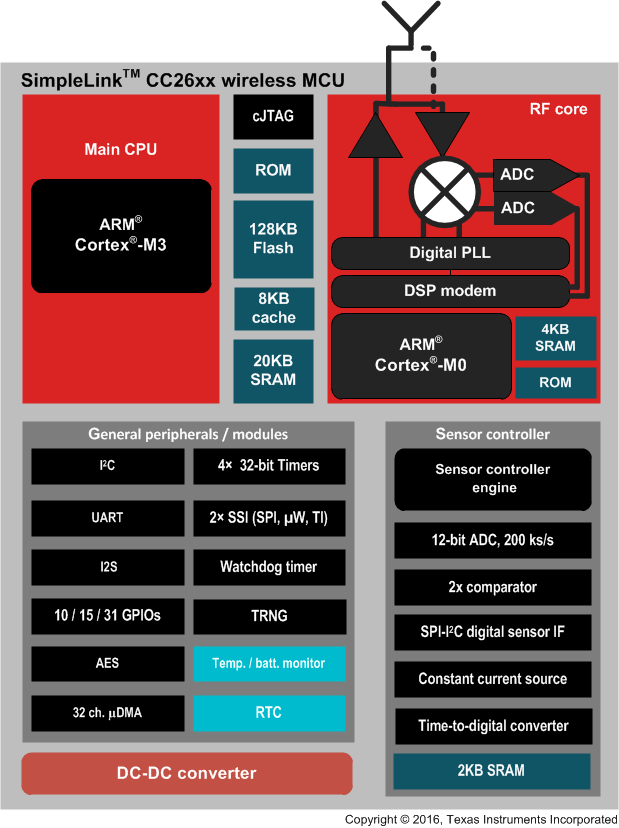
1.3.1 Functional Block Diagram
Figure 1-1 shows a block diagram for the CC2630.
 Figure 1-1 Block Diagram