SLPS455A January 2014 – August 2014 CSD88537ND
PRODUCTION DATA.
- 1Features
- 2Applications
- 3Description
- 4Revision History
- 5Specifications
- 6Device and Documentation Support
- 7Mechanical, Packaging, and Orderable Information
パッケージ・オプション
デバイスごとのパッケージ図は、PDF版データシートをご参照ください。
メカニカル・データ(パッケージ|ピン)
- D|8
サーマルパッド・メカニカル・データ
発注情報
1 Features
- Ultra-Low Qg and Qgd
- Avalanche Rated
- Pb Free
- RoHS Compliant
- Halogen Free
2 Applications
- Half Bridge for Motor Control
- Synchronous Buck Converter
3 Description
This dual SO-8, 60 V, 12.5 mΩ NexFET™ power MOSFET is designed to serve as a half bridge in low current motor control applications.
Top View
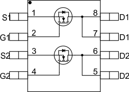
Product Summary
| TA = 25°C | TYPICAL VALUE | UNIT | ||
|---|---|---|---|---|
| VDS | Drain-to-Source Voltage | 60 | V | |
| Qg | Gate Charge Total (10 V) | 14 | nC | |
| Qgd | Gate Charge Gate-to-Drain | 2.3 | nC | |
| RDS(on) | Drain-to-Source On-Resistance | VGS = 6 V | 15 | mΩ |
| VGS = 10 V | 12.5 | mΩ | ||
| VGS(th) | Threshold Voltage | 3.0 | V | |
Ordering Information(1)
| Device | Media | Qty | Package | Ship |
|---|---|---|---|---|
| CSD88537ND | 13-Inch Reel | 2500 | SO-8 Plastic Package |
Tape and Reel |
| CSD88537NDT | 7-Inch Reel | 250 |
- For all available packages, see the orderable addendum at the end of the data sheet.
Absolute Maximum Ratings
| TA = 25°C | VALUE | UNIT | |
|---|---|---|---|
| VDS | Drain-to-Source Voltage | 60 | V |
| VGS | Gate-to-Source Voltage | ±20 | V |
| ID | Continuous Drain Current (Package limited) | 15 | A |
| Continuous Drain Current (Silicon limited), TC = 25°C | 16 | ||
| Continuous Drain Current (1) | 8.0 | ||
| IDM | Pulsed Drain Current, TA = 25°C(2) | 108 | A |
| PD | Power Dissipation(1) | 2.1 | W |
| TJ, Tstg |
Operating Junction and Storage Temperature Range |
–55 to 150 | °C |
| EAS | Avalanche Energy, single pulse ID = 32, L = 0.1 mH, RG = 25 Ω |
51 | mJ |
RDS(on) vs VGS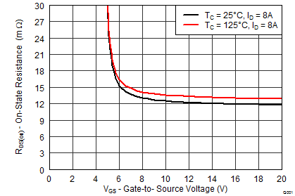 |
Gate Charge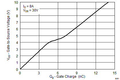 |