SNLS341C March 2011 – March 2015 DP83848Q-Q1
PRODUCTION DATA.
- 1 Device Overview
- 2 Revision History
- 3 Pin Configuration and Functions
- 4 Specifications
-
5 Detailed Description
- 5.1 Overview
- 5.2 Functional Block Diagram
- 5.3 Feature Description
- 5.4 Device Functional Modes
- 5.5
Programming
- 5.5.1
Architecture
- 5.5.1.1 100BASE-TX Transmitter
- 5.5.1.2
100BASE-TX Receiver
- 5.5.1.2.1 Analog Front End
- 5.5.1.2.2 Digital Signal Processor
- 5.5.1.2.3 Signal Detect
- 5.5.1.2.4 MLT-3 to NRZI Decoder
- 5.5.1.2.5 NRZI to NRZ
- 5.5.1.2.6 Serial to Parallel
- 5.5.1.2.7 Descrambler
- 5.5.1.2.8 Code-group Alignment
- 5.5.1.2.9 4B/5B Decoder
- 5.5.1.2.10 100BASE-TX Link Integrity Monitor
- 5.5.1.2.11 Bad SSD Detection
- 5.5.1.3
10BASE-T Transceiver Module
- 5.5.1.3.1 Operational Modes
- 5.5.1.3.2 Smart Squelch
- 5.5.1.3.3 Collision Detection and SQE
- 5.5.1.3.4 Carrier Sense
- 5.5.1.3.5 Normal Link Pulse Detection and Generation
- 5.5.1.3.6 Jabber Function
- 5.5.1.3.7 Automatic Link Polarity Detection and Correction
- 5.5.1.3.8 Transmit and Receive Filtering
- 5.5.1.3.9 Transmitter
- 5.5.1.3.10 Receiver
- 5.5.1
Architecture
- 5.6
Memory
- 5.6.1
Register Definition
- 5.6.1.1 Basic Mode Control Register (BMCR)
- 5.6.1.2 Basic Mode Status Register (BMSR)
- 5.6.1.3 PHY Identifier Register #1 (PHYIDR1)
- 5.6.1.4 PHY Identifier Register #2 (PHYIDR2)
- 5.6.1.5 Auto-Negotiation Advertisement Register (ANAR)
- 5.6.1.6 Auto-Negotiation Link Partner Ability Register (ANLPAR) (BASE Page)
- 5.6.1.7 Auto-Negotiation Link Partner Ability Register (ANLPAR) (Next Page)
- 5.6.1.8 Auto-Negotiate Expansion Register (ANER)
- 5.6.1.9 Auto-Negotiation Next Page Transmit Register (ANNPTR)
- 5.6.2
Extended Registers
- 5.6.2.1 PHY Status Register (PHYSTS)
- 5.6.2.2 False Carrier Sense Counter Register (FCSCR)
- 5.6.2.3 Receiver Error Counter Register (RECR)
- 5.6.2.4 100 Mb/s PCS Configuration and Status Register (PCSR)
- 5.6.2.5 RMII and Bypass Register (RBR)
- 5.6.2.6 LED Direct Control Register (LEDCR)
- 5.6.2.7 PHY Control Register (PHYCR)
- 5.6.2.8 10 Base-T Status/Control Register (10BTSCR)
- 5.6.2.9 CD Test and BIST Extensions Register (CDCTRL1)
- 5.6.2.10 Energy Detect Control (EDCR)
- 5.6.1
Register Definition
- 6 Application and Implementation
- 7 Power Supply Recommendations
- 8 Layout
- 9 Device and Documentation Support
- 10Mechanical, Packaging, and Orderable Information
パッケージ・オプション
メカニカル・データ(パッケージ|ピン)
- RTA|40
サーマルパッド・メカニカル・データ
- RTA|40
発注情報
1 Device Overview
1.1 Features
- AEC-Q100 Grade 2
- Extreme Temperature From –40°C to 105°C
- Low-Power 3.3-V, 0.18-µm CMOS Technology
- Low Power Consumption < 270 mW Typical
- 3.3-V MAC Interface
- Auto-MDIX for 10/100 Mb/s
- Energy Detection Mode
- 25-MHz Clock Out
- RMII Rev. 1.2 Interface (Configurable)
- MII Serial Management Interface (MDC and MDIO)
- IEEE 802.3u MII
- IEEE 802.3u Auto-Negotiation and Parallel Detection
- IEEE 802.3u ENDEC, 10BASE-T Transceivers and Filters
- IEEE 802.3u PCS, 100BASE-TX Transceivers and Filters
- Integrated ANSI X3.263 Compliant TP-PMD Physical Sublayer With Adaptive Equalization and Baseline Wander Compensation
- Error-Free Operation up to 150 Meters
- Programmable LED Support for Link and Activity
- Single Register Access for Complete PHY Status
- 10/100-Mb/s Packet BIST (Built in Self Test)
1.2 Applications
- Automotive and Transportation
- Industrial Controls and Factory Automation
- General Embedded Applications
1.3 Description
The number of applications requiring Ethernet connectivity continues to increase, driving Ethernet-enabled devices into harsher environments.
The DP83848Q-Q1 was designed to meet the challenge of these new applications with an extended temperature performance that goes beyond the typical Industrial temperature range. The DP83848Q-Q1 is a highly reliable, feature rich, robust device which meets IEEE 802.3u standards over an extended temperature range of –40°C to 105°C. This device is ideally suited for harsh environments such as automotive and transportation, wireless remote base stations, and industrial control applications.
The device offers enhanced ESD protection and the choice of an MII or RMII interface for maximum flexibility in MPU selection; all in a 40 pin WQFN package.
The DP83848Q-Q1 extends the leadership position of the PHYTER™ family of devices with a wide operating temperature range. The TI line of PHYTER transceivers builds on decades of Ethernet expertise to offer the high performance and flexibility that allows the end user an easy implementation tailored to meet these application needs.
Device Information(1)
| PART NUMBER | PACKAGE | BODY SIZE (NOM) |
|---|---|---|
| DP83848Q-Q1 | WQFN (40) | 6.00 mm × 6.00 mm |
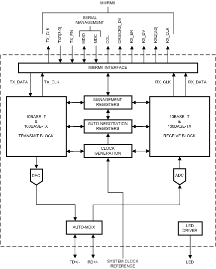
1.4 Functional Block Diagram
