SNLS450A January 2014 – June 2015 DS125DF111
PRODUCTION DATA.
- 1 Features
- 2 Applications
- 3 Description
- 4 Revision History
- 5 Pin Configuration And Functions
- 6 Specifications
-
7 Detailed Description
- 7.1 Overview
- 7.2 Functional Block Diagram
- 7.3 Feature Description
- 7.4 Device Functional Modes
- 7.5
Programming
- 7.5.1
SMBus Interface
- 7.5.1.1 Address Lines
- 7.5.1.2 Device Configuration in SMBus Slave Mode
- 7.5.1.3 Bit Fields in the Register Set
- 7.5.1.4 Writing To and Reading from the Control/Shared Registers
- 7.5.1.5 SMBus Strap Observation
- 7.5.1.6 Interrupt Channel Flag Bits
- 7.5.1.7 Control/Shared Register Reset
- 7.5.1.8 Device Revision and Device ID
- 7.5.1.9 Channel Select Register
- 7.5.1.10 Resetting Individual Channels of the Retimer
- 7.5.1.11 Rate and Subrate Setting
- 7.5.1.12 Overriding the CTLE Boost Setting
- 7.5.1.13 Overriding the Output Multiplexer
- 7.5.1.14 Overriding the VCO Divider Selection
- 7.5.1.15 Using the Internal Eye Opening Monitor
- 7.5.1.16 Overriding the DFE Tap Weights and Polarities
- 7.5.1.17 Enabling Slow Rise/Fall Time on the Output Driver
- 7.5.1.18 Using the PRBS Generator
- 7.5.1.19 Inverting the Output Polarity
- 7.5.1.20 Figure of Merit Adaption
- 7.5.1.21 Setting the Rate and Subrate for Lock Acquisition
- 7.5.1.22 Setting the Adaption/Lock Mode
- 7.5.1.23 Initiating Adaption
- 7.5.1.24 Overriding the CTLE Settings Used for CTLE Adaption
- 7.5.1.25 Setting the Output Differential Voltage
- 7.5.1.26 Setting the Output De-Emphasis Setting
- 7.5.1.27 CTLE Setting for Divide by 4 and Divide by 8 VCO Ranges
- 7.5.1
SMBus Interface
- 7.6 Register Maps
- 8 Application and Implementation
- 9 Power Supply Recommendations
- 10Layout
- 11Device and Documentation Support
- 12Mechanical, Packaging, and Orderable Information
パッケージ・オプション
メカニカル・データ(パッケージ|ピン)
- RTW|24
サーマルパッド・メカニカル・データ
- RTW|24
発注情報
1 Features
-
Pin Compatible Retimer Family
- DS110DF111 with DFE: 8.5 - 11.3 Gbps
- DS125DF111 with DFE: 9.8 - 12.5 Gbps
- Adaptive CTLE: 33 dB Max Boost at 6.25 GHz
- Self Tuning 5-Tap DFE
- Raw Equalized and Retimed Data Loopback
- Adjustable Transmit VOD: 600 to 1300 mVp-p
- Settable Tx De-Emphasis Driver 0 to –12dB
- Low Power Consumption: 220 mW/Channel
- Locks to Half/Quarter/Eighth Data Rates for Legacy Support
- On-Chip Eye Monitor (EOM), PRBS Generator
- Input Signal Detection, CDR Lock Detection/Indicator
- Single 3.3-V or 2.5-V Power Supply
- SMBus, EEPROM, or Pin Based Configuration
- 4-mm x 4-mm, 24-Pin WQFN Package
- Operating Temp Range: –40°C to 85°C
2 Applications
- Front Port Optical Interconnects
- SFF-8431
- 10G/1G Ethernet
- CPRI
3 Description
The DS125DF111 is a dual channel (1-lane bidirectional) retimer with integrated signal conditioning. The DS125DF111 includes an input Continuous-Time Linear Equalizer (CTLE), clock and data recovery (CDR) and transmit driver on each channel.
The DS125DF111 with its on-chip Decision Feedback Equalizer (DFE) can enhance the reach and robustness of long, lossy, cross-talk-impaired high speed serial links to achieve BER < 1x10–15. For less demanding applications/interconnects, the DFE can be switched off and achieve the same BER performance. The DS125DF111 and DS110DF111 devices are pin-compatible.
Each channel of the DS125DF111 independently locks to specific serial data at data rates from 9.8 to 12.5 Gbps or to any supported sub-rate of these data rates. This simplifies system design and lowers overall cost.
Programmable transmit de-emphasis driver offers precise settings to meet the SFF-8431 output eye template. The fully adaptive receive equalization (CTLE and DFE) enables longer distance transmission in lossy copper interconnect and backplanes with multiple connectors. The CDR function is ideal for use in front port parallel optical module applications to reset the jitter budget and retime high speed serial data.
Device Information(1)
| PART NUMBER | PACKAGE | BODY SIZE (NOM) |
|---|---|---|
| DS125DF111 | WQFN (24) | 4.0 mm × 4.0 mm |
- For all available packages, see the orderable addendum at the end of the datasheet.
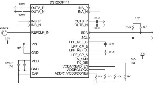
Typical Application
