SNOSCZ1B July 2015 – June 2016 LM74610-Q1
PRODUCTION DATA.
- 1 Features
- 2 Applications
- 3 Description
- 4 Revision History
- 5 Pin Configuration and Functions
- 6 Specifications
- 7 Detailed Description
- 8 Application and Implementation
- 9 Power Supply Recommendations
- 10Layout
- 11Device and Documentation Support
- 12Mechanical, Packaging, and Orderable Information
パッケージ・オプション
メカニカル・データ(パッケージ|ピン)
- DGK|8
サーマルパッド・メカニカル・データ
- DGK|8
発注情報
1 Features
- Qualified for Automotive Applications
- AEC-Q100 Qualified With the Following Results:
- Exceeds HBM ESD Classification Level 2
- Device CDM ESD Classification Level C4B
- Maximum reverse voltage of 45 V
- No Positive Voltage limitation to Anode Terminal
- Charge Pump Gate Driver for External N-Channel MOSFET
- Lower Power Dissipation than Schottky Diode/PFET Solutions
- Low Reverse Leakage Current
- Zero IQ
- Fast 2-µs Response to Reverse Polarity
- -40°C to +125°C Operating Ambient Temperature
- Can be Used in OR-ing Applications
- Meets CISPR25 EMI Specification
- Meets Automotive ISO7637 Transient Requirements with a Suitable TVS Diode
- No Peak Current Limit
2 Applications
- ADAS
- Infotainment Systems
- Power Tools (Industrial)
- Transmission Control Unit (TCU)
- Battery OR-ing Applications
3 Description
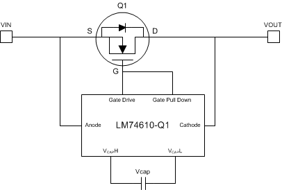
The LM74610-Q1 is a controller device that can be used with an N-Channel MOSFET in a reverse polarity protection circuitry. It is designed to drive an external MOSFET to emulate an ideal diode rectifier when connected in series with a power source. A unique advantage of this scheme is that it is not referenced to ground and thus has Zero Iq.
The LM74610-Q1 controller provides a gate drive for an external N-Channel MOSFET and a fast response internal comparator to discharge the MOSFET Gate in the event of reverse polarity. This fast pull-down feature limits the amount and duration of reverse current flow if opposite polarity is sensed. The device design also meets CISPR25 Class 5 EMI specifications and automotive ISO7637 transient requirements with a suitable TVS diode.
Device Information(1)
| PART NUMBER | PACKAGE | BODY SIZE (NOM) |
|---|---|---|
| LM74610-Q1 | VSSOP (8) | 3.00 mm x 5.00 mm |
Smart Diode Configuration

Application Diagram
