SCES531L December 2003 – May 2017 SN74AVC2T45
PRODUCTION DATA.
- 1 Features
- 2 Applications
- 3 Description
- 4 Revision History
- 5 Pin Configuration and Functions
-
6 Specifications
- 6.1 Absolute Maximum Ratings
- 6.2 ESD Ratings
- 6.3 Recommended Operating Conditions
- 6.4 Thermal Information
- 6.5 Electrical Characteristics
- 6.6 Switching Characteristics: VCCA = 1.2 V
- 6.7 Switching Characteristics: VCCA = 1.5 V ±0.1 V
- 6.8 Switching Characteristics: VCCA = 1.8 V ±0.15 V
- 6.9 Switching Characteristics: VCCA = 2.5 V ±0.2 V
- 6.10 Switching Characteristics: VCCA = 3.3 V ±0.3 V
- 6.11 Operating Characteristics
- 6.12
Typical Characteristics
- 6.12.1 Typical Propagation Delay (A to B) vs Load Capacitance, TA = 25°C, VCCA = 1.2 V
- 6.12.2 Typical Propagation Delay (A to B) vs Load Capacitance, TA = 25°C, VCCA = 1.5 V
- 6.12.3 Typical Propagation Delay (A-to-B) vs Load Capacitance, TA = 25°C, VCCA = 1.8 V
- 6.12.4 Typical Propagation Delay (A to B) vs Load Capacitance, TA = 25°C, VCCA = 2.5 V
- 6.12.5 Typical Propagation Delay (A to B) vs Load Capacitance, TA = 25°C, VCCA = 3.3 V
- 7 Parameter Measurement Information
- 8 Detailed Description
- 9 Application and Implementation
- 10Power Supply Recommendations
- 11Layout
- 12Device and Documentation Support
- 13Mechanical, Packaging, and Orderable Information
パッケージ・オプション
デバイスごとのパッケージ図は、PDF版データシートをご参照ください。
メカニカル・データ(パッケージ|ピン)
- DCU|8
- YZP|8
- DCT|8
サーマルパッド・メカニカル・データ
発注情報
1 Features
- Available in the Texas Instruments NanoFree™ Package
- VCC Isolation Feature: If Either VCC Input Is at GND, Both Ports Are in the High-Impedance State
- Dual Supply Rail Design
- I/Os Are 4.6-V Over Voltage Tolerant
- Ioff Supports Partial-Power-Down Mode Operation
- Max Data Rates
- 500 Mbps (1.8 V to 3.3 V)
- 320 Mbps (<1.8 V to 3.3 V )
- 320 Mbps (Level-Shifting to 2.5 V or 1.8 V)
- 280 Mbps (Level-Shifting to 1.5 V)
- 240 Mbps (Level-Shifting to 1.2 V)
- Latch-Up Performance Exceeds 100 mA Per JESD 78, Class II
- ESD Protection Exceeds JESD 22
2 Applications
- Smartphones
- Servers
- Desktop PCs and Notebooks
- Other Portable Devices
3 Description
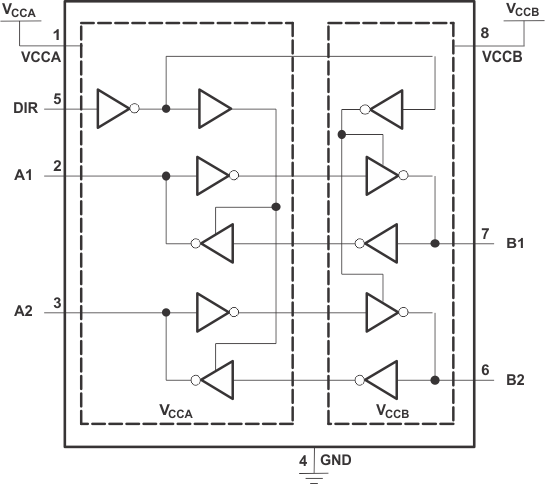
This 2-bit non-inverting bus transceiver uses two separate configurable power-supply rails. The A ports are designed to track VCCA and accepts any supply voltage from 1.2 V to 3.6 V. The B ports are designed to track VCCB and accepts any supply voltage from 1.2 V to 3.6 V. This allows for universal low-voltage bidirectional translation and level-shifting between any of the 1.2-V, 1.5-V, 1.8-V, 2.5-V, and 3.3-V voltage nodes.
The SN74AVC2T45 is designed for asynchronous communication between two data buses. The logic levels of the direction-control (DIR pin) input activate either the B-port outputs or the A-port outputs. The device transmits data from the A bus to the B bus when the B-port outputs are activated and from the B bus to the A bus when the A-port outputs are activated. The input circuitry on both A and B ports always is active and must have a logic HIGH or LOW level applied to prevent excess leakage current on the internal CMOS structure.
Device Information(1)
| PART NUMBER | PACKAGE | BODY SIZE (NOM) |
|---|---|---|
| SN74AVC2T45DCT | SM8 (8) | 2.95 mm × 2.80 mm |
| SN74AVC2T45DCU | VSSOP (8) | 2.30 mm × 2.00 mm |
| SN74AVC2T45YZP | DSBGA (8) | 1.89 mm × 0.89 mm |
- For all available packages, see the orderable addendum at the end of the data sheet.
