SCLS469F March 2003 – December 2014 SN74LV4052A-Q1
PRODUCTION DATA.
- 1 Features
- 2 Applications
- 3 Description
- 4 Revision History
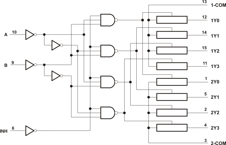
- 5 Pin Configuration and Functions
- 6 Specifications
- 7 Parameter Measurement Information
- 8 Detailed Description
- 9 Application and Implementation
- 10Power Supply Recommendations
- 11Layout
- 12Device and Documentation Support
- 13Mechanical, Packaging, and Orderable Information
パッケージ・オプション
メカニカル・データ(パッケージ|ピン)
サーマルパッド・メカニカル・データ
- D|16
発注情報
1 Features
- Qualified for Automotive Applications
- AEC-Q100 Qualified With the Following Results:
- Device Temperature Grade 1: –40°C to +125°C Ambient Operating Temperature Range
- Device HBM ESD Classification Level 2
- Device CDM ESD Classification Level C4B
- Supports Mixed-Mode Voltage Operation on All Ports
- Fast Switching
- High On-Off Output-Voltage Ratio
- Low Crosstalk Between Switches
- Extremely Low Input Current
2 Applications
- Automotive:
- Signal Gating
- Chopping
- Modulation or Demodulation (Modem)
- Signal Multiplexing for Analog-to-Digital and Digital-to-Analog Conversion Systems
3 Description
These dual 4-channel CMOS analog multiplexers and demultiplexers are designed for 2-V to 5.5-V VCC operation.
The SN7LV4052A-Q1 devices handle both analog and digital signals. Each channel permits signals with amplitudes up to 5.5 V (peak).
Applications include signal gating, chopping, modulation or demodulation (modem), and signal multiplexing for analog-to-digital and digital-to-analog conversion systems.
Device Information(1)
| PART NUMBER | PACKAGE | BODY SIZE (NOM) |
|---|---|---|
| SN74LV4052A-Q1 | TSSOP (16) | 5.00 mm × 4.40 mm |
| SOIC (16) | 9.90 mm × 3.91 mm |
- For all available packages, see the orderable addendum at the end of the datasheet.
Logic Diagram (Positive Logic)