SCES223T April 1999 – October 2014 SN74LVC1G125
PRODUCTION DATA.
- 1 Features
- 2 Applications
- 3 Description
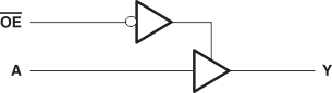
- 4 Simplified Schematic
- 5 Revision History
- 6 Pin Configuration and Functions
-
7 Specifications
- 7.1 Absolute Maximum Ratings
- 7.2 Handling Ratings
- 7.3 Recommended Operating Conditions
- 7.4 Thermal Information
- 7.5 Electrical Characteristics
- 7.6 Switching Characteristics, CL = 15 pF
- 7.7 Switching Characteristics, -40°C to 85°C
- 7.8 Switching Characteristics, -40°C to 125°C
- 7.9 Operating Characteristics
- 7.10 Typical Characteristics
- 8 Parameter Measurement Information
- 9 Detailed Description
- 10Application and Implementation
- 11Power Supply Recommendations
- 12Layout
- 13Device and Documentation Support
- 14Mechanical, Packaging, and Orderable Information
1 Features
- Available in the Ultra Small 0.64-mm2
Package (DPW) With 0.5-mm Pitch - Supports 5-V VCC Operation
- Inputs Accept Voltages to 5.5 V
- Provides Down Translation to VCC
- Max tpd of 3.7 ns at 3.3 V
- Low Power Consumption, 10-μA Max ICC
- ±24-mA Output Drive at 3.3 V
- Ioff Supports Live Insertion, Partial-Power-Down Mode, and Back-Drive Protection
- Latch-Up Performance Exceeds 100 mA
Per JESD 78, Class II - ESD Protection Exceeds JESD 22
- 2000-V Human-Body Model (A114-A)
- 200-V Machine Model (A115-A)
- 1000-V Charged-Device Model (C101)
2 Applications
- Cable Modem Termination System
- High-Speed Data Acquisition and Generation
- Military: Radar and Sonar
- Motor Control: High-Voltage
- Power Line Communication Modem
- SSD: Internal or External
- Video Broadcasting and Infrastructure:
Scalable Platform - Video Broadcasting: IP-Based Multi-Format Transcoder
- Video Communications System
3 Description
This bus buffer gate is designed for 1.65-V to 5.5-V VCC operation.
The SN74LVC1G125 device is a single line driver with a 3-state output. The output is disabled when the output-enable (OE) input is high.
The CMOS device has high output drive while maintaining low static power dissipation over a broad VCC operating range.
The SN74LVC1G125 device is available in a variety of packages including the ultra-small DPW package with a body size of 0.8 mm × 0.8 mm.
Device Information(1)
| DEVICE NAME | PACKAGE | BODY SIZE (NOM) |
|---|---|---|
| SN74LVC1G125 | SOT-23 (5) | 2.90 mm × 1.60 mm |
| SC70 (5) | 2.00 mm × 1.25 mm | |
| SON (6) | 1.45 mm × 1.00 mm | |
| DSBGA (5) | 1.40 mm × 0.90 mm | |
| X2SON (4) | 0.80 mm × 0.80 mm |
- For all available packages, see the orderable addendum at the end of the data sheet.
4 Simplified Schematic