SLVSCI4B February 2014 – September 2014 TPS22961
PRODUCTION DATA.
- 1 Features
- 2 Applications
- 3 Description
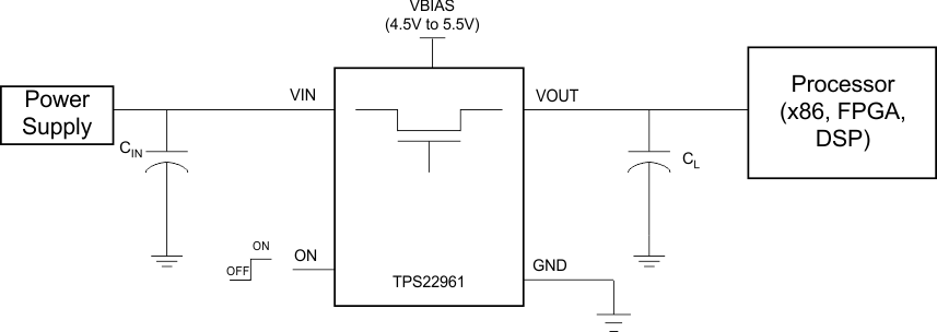
- 4 Simplified Schematic
- 5 Revision History
- 6 Terminal Configuration and Functions
- 7 Specifications
- 8 Detailed Description
- 9 Applications and Implementation
- 10Power Supply Recommendations
- 11Layout
- 12Device and Documentation Support
- 13Mechanical, Packaging, and Orderable Information
パッケージ・オプション
デバイスごとのパッケージ図は、PDF版データシートをご参照ください。
メカニカル・データ(パッケージ|ピン)
- DNY|8
サーマルパッド・メカニカル・データ
発注情報
1 Features
- Integrated Single Channel Load Switch
- VBIAS Voltage Range: 3 V to 5.5 V
- Input Voltage Range: 0.8 V to 3.5 V
- Ultra low RON Resistance
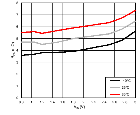
- RON = 4.4 mΩ at VIN = 1.05 V (VBIAS = 5 V)
- 6A Maximum Continuous Switch Current
- Low Quiescent Current < 1 µA (max)
- Low Control Input Threshold Enables use of 1.2-V/1.8-V/2.5-V/3.3-V Logic
- Controlled Slew Rate
- tR = 4.2 µs at VIN = 1.05 V (VBIAS = 5 V)
- Quick Output Discharge (QOD)
- SON 8-terminal Package with Thermal Pad
- ESD Performance Tested per JESD 22
- 2-kV HBM and 1-kV CDM
2 Applications
- Ultrabook™/Notebooks
- Desktops
- Servers
- Set-top Boxes
- Telecom Systems
- Tablet PC
3 Description
The TPS22961 is a small, ultra-low RON, single channel load switch with controlled turn on. The device contains an N-channel MOSFET that can operate over an input voltage range of 0.8 V to 3.5 V and supports a maximum continuous current of 6 A.
The combination of ultra-low RON and high current capability of the device makes it ideal for driving processor rails with very tight voltage dropout tolerances. Quick rise time of the device allows for power rails to come up quickly when the device is enabled, thereby reducing response time for power distribution. The switch can be independently controlled via the ON terminal, which is capable of interfacing directly with low-voltage control signals originating from microcontrollers or low voltage discrete logic. The device further reduces the total solution size by integrating a 260 Ω pull-down transistor for quick output discharge (QOD) when the switch is turned off.
The TPS22961 is available in a small, space-saving 3 mm x 3 mm 8-SON package (DNY) with integrated thermal pad allowing for high power dissipation. The device is characterized for operation over the free-air temperature range of –40°C to 85°C.
Device Information(1)
| PART NUMBER | PACKAGE | BODY SIZE |
|---|---|---|
| TPS22961 | WSON (8) | 3.00 mm x 3.00 mm |
- For all available packages, see the orderable addendum at the end of the datasheet.
4 Simplified Schematic
RON vs VIN (VBIAS = 5 V, IOUT = –200 mA)