SLVSBE9E April 2012 – June 2015 TPS27081A
PRODUCTION DATA.
- 1 Features
- 2 Applications
- 3 Description
- 4 Revision History
- 5 Pin Configuration and Functions
- 6 Specifications
- 7 Detailed Description
-
8 Application and Implementation
- 8.1 Application Information
- 8.2 Typical Application
- 8.3
System Examples
- 8.3.1 Standby Power Isolation
- 8.3.2 Boost Regulator With True Shutdown
- 8.3.3 Single Module Multiple Power Supply Sequencing
- 8.3.4 Multiple Modules Interdependent Power Supply Sequencing
- 8.3.5 TFT LCD Module Inrush Current Control
- 8.3.6 Multiple Modules Interdependent Supply Sequencing Without a GPIO Input
- 9 Power Supply Recommendations
- 10Layout
- 11Device and Documentation Support
- 12Mechanical, Packaging, and Orderable Information
1 Features
-
Low ON-Resistance, High-Current PFET
- RDS(on) = 32 mΩ at VGS = –4.5 V
- RDS(on) = 44 mΩ at VGS = –3 V
- RDS(on) = 82 mΩ at VGS = –1.8 V
- RDS(on) = 93 mΩ at VGS = –1.5 V
- RDS(on) = 155 mΩ at VGS = –1.2 V
- Adjustable Turnon and Turnoff Slew Rate Control Through External R1, R2, and C1
- Supports a Wide Range of 1.2-V to 8-V Supply Inputs
- Integrated NMOS for PFET Control
- NMOS ON/OFF Supports a Wide Range of 1-V to 8-V Control Logic Interface
- Full ESD Protection (All Pins)
- HBM 2 kV, CDM 500 V
- Ultra-Low Leakage Current in Standby (Typical 100 nA)
- Available in Tiny 6-Pin Package
- 2.9 mm × 2.8 mm × 0.75 mm SOT (DDC)
2 Applications
- High-Side Load Switches
- Inrush Current Control
- Power Sequencing and Control
- Standby Power Isolation
- Portable Power Switches
3 Description
The TPS27081A device is a high-side load switch that integrates a Power PFET and a Control NFET in a tiny package.
The TPS27081A features industry-standard ESD protection on all pins providing better ESD compatibility with other onboard components.
The TPS27081A level shifts ON/OFF logic signal to VIN levels and supports as low as 1-V CPU or MCU logic to control higher voltage power supplies without requiring an external level-shifter.
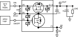
Switching a large value output capacitor CL through a fast ON/OFF logic signal may result in an excessive inrush current. To control the load inrush current, connect a resistor R2 and add an external capacitor C1 as shown in the Simplified Schematic. To configure the TPS27081A to achieve a specific slew rate, refer to the Application and Implementation section.
A single pullup resistor R1 is required in standby power switch applications. In such applications connect the R2 pin of the TPS27081A to the system ground when inrush current control is not required.
Device Information(1)
| PART NUMBER | PACKAGE | BODY SIZE (NOM) |
|---|---|---|
| TPS27081A | SOT (6) | 2.90 mm × 1.60 mm |
- For all available packages, see the orderable addendum at the end of the data sheet.
Simplified Schematic
