SLVS806D April 2009 – December 2015 TPS61240 , TPS61241
PRODUCTION DATA.
- 1 Features
- 2 Applications
- 3 Description
- 4 Revision History
- 5 Device Options
- 6 Pin Configuration and Functions
- 7 Specifications
- 8 Parameter Measurement Information
- 9 Detailed Description
- 10Application and Implementation
- 11Power Supply Recommendations
- 12Layout
- 13Device and Documentation Support
- 14Mechanical, Packaging, and Orderable Information
パッケージ・オプション
メカニカル・データ(パッケージ|ピン)
サーマルパッド・メカニカル・データ
- DRV|6
発注情報
1 Features
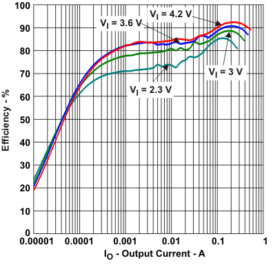
- Efficiency > 90% at Nominal Operating Conditions
- Total DC Output Voltage Accuracy 5.0 V±2%
- Typical 30-μA Quiescent Current
- Best in Class Line and Load Transient
- Wide VIN Range From 2.3 V to 5.5 V
- Output Current up to 450 mA
- Automatic PFM/PWM Mode Transition
- Low Ripple Power Save Mode for Improved Efficiency at Light Loads
- Internal Softstart, 250-μs Typical Start-Up Time
- 3.5-MHz Typical Operating Frequency
- Load Disconnect During Shutdown
- Current Overload and Thermal Shutdown Protection
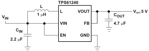
- Three Surface-Mount External Components Required (One MLCC Inductor, Two Ceramic Capacitors)
- Total Solution Size <13 mm2
- Available in a 6-Pin DSBGA and 2-mm × 2-mm WSON Package
2 Applications
- USB-OTG Applications
- Portable HDMI Applications
- Cell Phones, Smart Phones
- PDAs, Pocket PCs
- Portable Media Players
- Digital Cameras
3 Description
The TPS6124x device is a highly efficient synchronous step-up DC-DC converter optimized for products powered by either a three-cell alkaline, NiCd or NiMH, or one-cell Li-Ion or Li-Polymer battery. The TPS6124x supports output currents up to 450 mA. The TPS61240 has an input valley current limit of 500 mA, and the TPS61241 has an input valley current of 600 mA.
With an input voltage range of 2.3 V to 5.5 V, the device supports batteries with extended voltage range and are ideal to power portable applications like mobile phones and other portable equipment. The TPS6124x boost converter is based on a quasi-constant on-time valley current mode control scheme.
The TPS6124x presents a high impedance at the VOUT pin when shut down. This allows for use in applications that require the regulated output bus to be driven by another supply while the TPS6124x is shut down.
During light loads the device will automatically pulse skip allowing maximum efficiency at lowest quiescent currents. In the shutdown mode, the current consumption is reduced to less than 1 μA.
TPS6124x allows the use of small inductors and capacitors to achieve a small solution size. During shutdown, the load is completely disconnected from the battery. The TPS6124x is available in a 6-pin DSBGA and 2-mm × 2-mm WSON package.
Device Information(1)
| PART NUMBER | PACKAGE | BODY SIZE (NOM) |
|---|---|---|
| TPS61240 | WSON (6) | 2.00 mm × 2.00 mm |
| DSBGA (6) | 1.25 mm × 0.86 mm | |
| TPS61241 | DSBGA (6) | 1.25 mm × 0.86 mm |
- For all available packages, see the orderable addendum at the end of the datasheet.
Typical Application Schematic

Efficiency vs Output Current
