SWRS116F August 2011 – October 2014 CC1175
PRODUCTION DATA.
- 1 Device Overview
- 2Revision History
- 3Terminal Configuration and Functions
-
4Specifications
- 4.1 Absolute Maximum Ratings
- 4.2 Handling Ratings
- 4.3 Recommended Operating Conditions (General Characteristics)
- 4.4 Thermal Resistance Characteristics for RHB Package
- 4.5 RF Characteristics
- 4.6 Regulatory Standards
- 4.7 Current Consumption, Static Modes
- 4.8 Current Consumption, Transmit Modes
- 4.9 Transmit Parameters
- 4.10 PLL Parameters
- 4.11 Wake-up and Timing
- 4.12 High-Speed Crystal Oscillator
- 4.13 High-Speed Clock Input (TCXO)data to TCXO table
- 4.14 32-kHz Clock Input
- 4.15 Low-Speed RC Oscillator
- 4.16 I/O and Reset
- 4.17 Temperature Sensor
- 4.18 Typical Characteristics
- 5Detailed Description
- 6Typical Application Circuit
- 7Device and Documentation Support
- 8Mechanical Packaging and Orderable Information
パッケージ・オプション
メカニカル・データ(パッケージ|ピン)
- RHB|32
サーマルパッド・メカニカル・データ
- RHB|32
発注情報
1 Device Overview
1.1 Features
- High-Performance, Single-Chip Transmitter
- Very Low Phase Noise: –111 dBc/Hz at
10-kHz Offset
- Very Low Phase Noise: –111 dBc/Hz at
- High Spectral Efficiency (9.6 kbps in 12.5-kHz Channel in Compliance With FCC Narrowbanding Mandate)
- 128-Byte TX FIFO
- Support for Seamless Integration With the CC1190 Device for Increased Range Giving up to +27-dBm Output Power
- Programmable Output Power up to +16 dBm With 0.4-dB Step Size
- Power Supply
- Wide Supply Voltage Range (2.0 V to 3.6 V)
- Low Current Consumption:
- TX: 45 mA at +14 dBm
- Power Down: 0.12 μA (0.5 μA With Timer Running)
- Automatic Output Power Ramping
- Configurable Data Rates: 0 to 200 kbps
- Supported Modulation Formats: 2-FSK,
2-GFSK, 4-FSK, 4-GFSK, MSK, OOK - RoHS-Compliant 5-mm x 5-mm No-Lead QFN 32-Pin Package (RHB)
- Regulations – Suitable for Systems Targeting Compliance With
- Europe: ETSI EN 300 220, ETSI EN 54-25
- US: FCC CFR47 Part 15, FCC CFR47 Part 90, 24, and 101
- Japan: ARIB RCR STD-T30, ARIB STD-T67, ARIB STD-T108
- Peripherals and Support Functions
- TCXO Support and Control, also in Power Modes
- Optional Coding Gain Feature for Increased Range and Robustness
- Temperature Sensor
1.2 Applications
- One-way Narrowband Ultra-Low Power Wireless Systems With Channel Spacing Down to 6.25 kHz
- 169-, 315-, 433-, 868-, 915-, 920-, 950-MHz ISM/SRD Band Systems
- Wireless Metering and Wireless Smart Grid (AMR and AMI)
- IEEE 802.15.4g Systems
- Home and Building Automation
- Wireless Alarm and Security Systems
- Industrial Monitoring and Control
- Wireless Healthcare Applications
- Wireless Sensor Networks and Active RFID
1.3 Description
The CC1175 device is a fully integrated single-chip radio transmitter designed for high performance at very low-power and low-voltage operation in cost-effective wireless systems. All filters are integrated, thus removing the need for costly external SAW and IF filters. The device is mainly intended for the ISM (Industrial, Scientific, and Medical) and SRD (Short Range Device) frequency bands at 164–192 MHz, 274–320 MHz, 410–480 MHz, and 820–960 MHz.
The CC1175 device provides extensive hardware support for packet handling, data buffering, and burst transmissions. The main operating parameters of the CC1175 device can be controlled through an SPI interface. In a typical system, the CC1175 device will be used with a microcontroller and only a few external passive components.
1.4 Functional Block Diagram
Figure 1-1 shows the system block diagram of the CC1175 device.
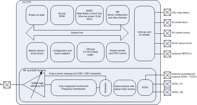 Figure 1-1 Functional Block Diagram