SLLS853F August 2007 – January 2015 DAC5682Z
PRODUCTION DATA.
- 1 Features
- 2 Applications
- 3 Description
- 4 Revision History
- 5 Description (continued)
- 6 Pin Configuration and Functions
- 7 Specifications
-
8 Detailed Description
- 8.1 Overview
- 8.2 Functional Block Diagram
- 8.3
Feature Description
- 8.3.1 FIR Filters
- 8.3.2 Coarse Mixers: CMIX0 and CMIX1
- 8.3.3 Clock Inputs
- 8.3.4 LVDS Data Interfacing
- 8.3.5 LVDS Inputs
- 8.3.6 LVDS SYNCP/N Operation
- 8.3.7 DLL Operation
- 8.3.8 CMOS Digital Inputs
- 8.3.9 Reference Operation
- 8.3.10 DAC Transfer Function
- 8.3.11 DAC Output SINC Response
- 8.3.12 Analog Current Outputs
- 8.3.13 Designing the PLL Loop Filter
- 8.3.14 Test Methodology
- 8.4 Device Functional Modes
- 8.5 Programming
- 8.6
Register Maps
- 8.6.1 Register Name: STATUS0 - Address: 0x00, Default = 0x03
- 8.6.2 Register Name: CONFIG1 - Address: 0x01, Default = 0x10
- 8.6.3 Register Name: CONFIG2 - Address: 0x02, Default = 0xC0
- 8.6.4 Register Name: CONFIG3 - Address: 0x03, Default = 0x70
- 8.6.5 Register Name: STATUS4 - Address: 0x04, Default = 0x00
- 8.6.6 Register Name: CONFIG5 - Address: 0x05, Default = 0x00
- 8.6.7 Register Name: CONFIG6 - Address: 0x06, Default = 0x0C
- 8.6.8 Register Name: CONFIG7 - Address: 0x07, Default = 0xFF
- 8.6.9 Register Name: CONFIG8 - Address: 0x08, Default = 0x00
- 8.6.10 Register Name: CONFIG9 - Address: 0x09, Default = 0x00
- 8.6.11 Register Name: CONFIG10 - Address: 0x0A, Default = 0x00
- 8.6.12 Register Name: CONFIG11 - Address: 0x0B, Default = 0x00
- 8.6.13 Register Name: CONFIG12 - Address: 0x0C, Default = 0x00
- 8.6.14 Register Name: CONFIG13 - Address: 0x0D, Default = 0x00
- 8.6.15 Register Name: CONFIG14 - Address: 0x0E, Default = 0x00
- 8.6.16 Register Name: CONFIG15 - Address: 0x0F, Default = 0x00
- 9 Application and Implementation
- 10Power Supply Recommendations
- 11Layout
- 12Device and Documentation Support
- 13Mechanical, Packaging, and Orderable Information
パッケージ・オプション
デバイスごとのパッケージ図は、PDF版データシートをご参照ください。
メカニカル・データ(パッケージ|ピン)
- RGC|64
サーマルパッド・メカニカル・データ
- RGC|64
発注情報
1 Features
- 16-Bit Digital-to-Analog Converter (DAC)
- 1.0 GSPS Update Rate
- 16-Bit Wideband Input LVDS Data Bus
- 8 Sample Input FIFO
- Interleaved I/Q Data for Dual-DAC Mode
- High Performance
- 73-dBc ACLR WCDMA TM1 at 180 MHz
- 2x-32x Clock Multiplying PLL/VCO
- 2x or 4x Interpolation Filters
- Stopband Transition 0.4 to 0.6 Fdata
- Filters Configurable in Either Low-Pass or High-Pass Mode
- Allows Selection of Higher Order Image
- Fs/4 Coarse Mixer
- On-Chip 1.2-V Reference
- Differential Scalable Output: 2 to 20 mA
- Package: 64-Pin 9-mm × 9-mm QFN
2 Applications
- Cellular Base Stations
- Broadband Wireless Access (BWA)
- WiMAX 802.16
- Fixed Wireless Backhaul
- Cable Modem Termination System (CMTS)
3 Description
The DAC5682Z is a dual-channel 16-bit 1.0 GSPS DAC with wideband LVDS data input, integrated 2x/4x interpolation filters, onboard clock multiplier, and internal voltage reference. The DAC5682Z offers superior linearity, noise, crosstalk, and PLL phase noise performance.
The DAC5682Z integrates a wideband LVDS port with on-chip termination. Full-rate input data can be transferred to a single DAC channel, or half-rate and 1/4-rate input data can be interpolated by onboard 2x or 4x FIR filters. Each interpolation FIR is configurable in either low-pass or high-pass mode, allowing selection of a higher order output spectral image. An on-chip delay lock loop (DLL) simplifies LVDS interfacing by providing skew control for the LVDS input data clock.
Device Information(1)
| PART NUMBER | PACKAGE | BODY SIZE (NOM) |
|---|---|---|
| DAC5682Z | VQFN (64) | 9.00 mm × 9.00 mm |
- For all available packages, see the orderable addendum at the end of the data sheet.
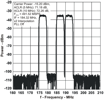
3-Carrier WCDMA TM1 With a Gap
4 Revision History
Changes from E Revision (August 2012) to F Revision
- Added ESD Ratings table, Feature Description section, Device Functional Modes, Application and Implementation section, Power Supply Recommendations section, Layout section, Device and Documentation Support section, and Mechanical, Packaging, and Orderable Information sectionGo
Changes from D Revision (February 2011) to E Revision
- Changed the Revision to E, August 2012Go
- Changed the graphic entity of Figure 30 for clarification.Go
- Changed the first paragraph of ANALOG CURRENT OUTPUTS section for clarification.Go
Changes from C Revision (November 2008) to D Revision
- Changed "defined by individual control bits in registers CONFIG1, CONFIG5 and CONFIG6." to "defined by individual control bits in registers CONFIG1 and CONFIG5."Go
- Changed wording in second sentence of RECOMMENED....PROCEDURE section from CONFIG5 clkdiv_sync_dis and FIFO_sync_dis bits as well to CONFIG5 clkdiv_sync_dis as wellGo
- Deleted list items in first and second ordered list in RECOMMENED....PROCEDURE section Go
- Changed CONFIG5 Bit4 from "FIFO_ sync_dis" to "Reserved" in Register MapGo
- Changed CONFIG6 Bit 7 from "Hold_ sync_dis" to "Reserved" in Register MapGo
- Deleted - unless-----CONFIG5 register. in FIFO_offset(2:0): on page 21Go
- Changed Bit 4 in CONFIG5 table from FIFO_sync_dis to ReservedGo
- Changed "FIFO_sync_sis: Disables the FIFO offset sync........ CONFIG1 register" to "Reserved (Bit 4): Set to 0 for proper operation."Go
- Changed Hold_sync _dis to ReservedGo
- Changed from Hold_sync_dis: When set, disables the sync to the FIFO .....control bit in CONFIG5." to " Reserved (Bit 7): Set to 0 for proper operation."Go
Changes from B Revision (April 2008) to C Revision
- Changed Thermal Conductivity θJA (still air) from 22 to 20Go
- Changed θJC from 7 to 0.2Go
- Changed θJP from 0.2 to 3.5Go
- Changed DC Spec - Analog Output test condition from "without internal reference"Go
- Changed DC spec. REFERENCE INPUT, Small signal bandwidth conditionsGo
- Changed Power Supply DVDD MIN from 1.71 to 1.7 and MAX from 2.15 to 1.9Go
- Changed Power Supply CLKVDD MIN from 1.71 to 1.7 and MAX from 2.15 to 1.9Go
- Added "DC tested" to PSRR spec.Go
- Added Digital latency spec.Go
- Added Power-up time specGo
- Added D[15:0]P/NGo
- Changed VITH+ specGo
- Changed VITH– specGo
- Changed IIH and IIL spec from –40 MIN and +40 MAX to ±20 TYPGo
- Changed t(SCLK) term to t(SCLKL) for Low time of SCLKGo
- Changed Clock Input Differential voltage from 0.5V to 0.4V MIN and added footnoteGo
- Added explanatory paragraph for LVDS Inputs; prior to Figure 33Go
- Changed Figure 34 waveform label VA,B calloutGo
- Added explanatory paragraph for Figure 35.Go
- Changed calculation for C2 Designing the PLL Loop FilterGo
- Added URL link to calculator file.Go
- Changed last sentence of Dual-Channel Real Upconversion paragraph.Go
- Added modes to Dual-Channel Real Upconversion OptionsGo
- Added references to CDCE62005 (3 places) Go
- Added Multi-DAC Synchronization ProcedureGo
- Changed Recommended DAC Startup SequenceGo
Changes from A Revision (September 2007) to B Revision
- Changed tr(IOUT) spec. output rise time 10% to 90% typical value from 2 ns to 220 psGo
- Changed tf(IOUT) spec. output fall time 10% to 90% typical value from 2 ns to 220 psGo
- Changed ZT spec. internal termination from 100 Ω min, 120 Ω max; to 85 Ω min, 135 Ω maxGo
- Deleted temperature deratings for fDATA specificationsGo
- Added DLL operating frequency range specificationsGo
- Changed In-Band SFDR vs IF, Figure 6Go
- Changed CAC values from 0.1 to 0.01μF, Figure 30Go
- Changed capacitor values from 0.1 to 0.01μF, Figure 35Go
Changes from * Revision (August 2007) to A Revision
- Changed from product preview to production dataGo