SLRS065E September 2013 – November 2015 DRV8860
PRODUCTION DATA.
- 1 Features
- 2 Applications
- 3 Description
- 4 Simplified Schematic
- 5 Revision History
- 6 Pin Configuration and Functions
- 7 Specifications
- 8 Detailed Description
- 9 Application and Implementation
- 10Power Supply Recommendations
- 11Layout
- 12Device and Documentation Support
- 13Mechanical, Packaging, and Orderable Information
パッケージ・オプション
メカニカル・データ(パッケージ|ピン)
サーマルパッド・メカニカル・データ
- PWP|16
発注情報
1 Features
- 8-Channel Protected Low-side Driver
- Continuous Current Driving Capability
- 560 mA (Single Channel on) PW and PWP
- 200 mA (8 Channels on) PW
- 330 mA (8 Channels on) PWP
- Support Parallel Configuration
- 8 V to 38 V Supply Voltage Range
- Input Digital Noise Filter for Noise Immunity
- Internal Data Read Back Capability for Reliable Control
- Protection and Diagnostic Features
- Overcurrent Protection (OCP)
- Open Load Detection (OL)
- Overtemperature Shutdown (OTS)
- Undervoltage Lockout (UVLO)
- Individual Channel Status Report
- Fault Condition Alarm
2 Applications
3 Description
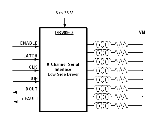
The DRV8860 provides an 8-channel low side driver with overcurrent protection and open/shorted load detection. It has built-in diodes to clamp turn-off transients generated by inductive loads, and can be used to drive unipolar stepper motors, DC motors, relays, solenoids, or other loads.
The PWP package can supply up to 330 mA × 8 channel and The PW package can supply up to 200 mA × 8 channel continuous output current. A single channel can deliver up to 560 mA continuous output current.
A serial interface is provided to control the DRV8860 output drivers, configure internal setting register and read the fault status of each channel. DRV8860 devices can be daisy-chained together to use a single serial interface. Energizing-time and holding-PWM-Duty cycles are configurable through serial interface as well. These functions allow for cooler running than always-on solutions.
Internal shutdown functions are provided for overcurrent protection, short-circuit protection, undervoltage lockout, and overtemperature. DRV8860A does not include open load detection. Fault information for each channel can be read out through serial interface and indicated by an external fault pin.
Device Information(1)
| PART NUMBER | PACKAGE | BODY SIZE (NOM) |
|---|---|---|
| DRV8860 | TSSOP (16) | 5.00 mm × 6.40 mm |
| HTSSOP (16) | 5.00 mm × 4.40 mm | |
| DRV8860A | TSSOP (16) | 5.00 mm × 6.40 mm |
- For all available packages, see the orderable addendum at the end of the datasheet.
4 Simplified Schematic

