SBAA529 March 2022 AMC23C14
Design Goals
| Overvoltage Level | Undervoltage Level | Low-Side VDD | High-Side VDD | Transient Response Time |
|---|---|---|---|---|
| 28.8 V | 20.4 V | 2.7 V–5.5 V | 24 V | 360 ns |
Design Description
This high-speed, isolated undervoltage and overvoltage detection circuit is implemented with a dual isolated window comparator with an adjustable threshold (AMC23C14). This circuit is designed for industrial field-supply applications where the controller-side must detect whether the remote module supply voltage is in a valid range.
The AMC23C14 is selected for its robust reinforced isolation with a high CMTI of 100 kV/μs (minimum), the adjustable dual window comparator thresholds, a wide high-side supply voltage range (3 V to 27 V), and the extended industrial temperature range (–40°C to +125°C).
Design Notes
- To minimize errors, choose precision resistors for the voltage divider (R5 and R6) and the threshold-setting resistor (R1).
- The AMC23C14 is powered from the field supply and is protected against voltage > 30 V (absolute maximum supply) by a Zener diode and shunt resistor.
- Select the voltage divider and threshold-setting resistors based on the desired operating voltage range.
Design Steps
- Determine the voltage divider ratio needed to
trip the fixed internal 300-mV threshold when the power supply exceeds the
minimum valid operating voltage of 20.4 (24 V – 15%). Size the total resistance
of the voltage divider to set its current at 100 μA when the Vsupp is
at the desired operating voltage of 24 V.
Solving the system of equations results in R5 = 236 kΩ, R6 = 3.52 kΩ.
- Using the Analog Engineer's Calculator, the closest E96 resistor value is 237 kΩ and 3.48 kΩ.
- Size the threshold-setting resistor to trip the
adjustable-threshold comparator when the power supply exceeds 28.8 V (24 V +
20%).
- Select a 27-V Zener diode to protect the AMC23C14 from voltages greater than the recommended operating supply voltage.
Design Simulations
The following images are SPICE simulation waveforms of the undervoltage and overvoltage detection circuit. Included is the VDD1 input, which shows the Zener diode protects the VDD1 input from voltages outside of its operating range. SPICE Simulation of the Undervoltage and Overvoltage Detection Circuit - Rising shows the Spice simulation with the output trigger points on a rising input voltage. SPICE Simulation of the Undervoltage and Overvoltage Detection Circuit - Falling shows a similar image but with the output trigger points on a falling input voltage. Comparing the two figures, the trigger points differ by 0.3 V with the falling voltage input having a lower trigger value.
Measured Response
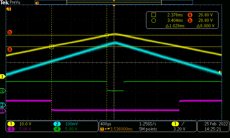
The following images show the measured output of the undervoltage and overvoltage detection circuit, comparing the outputs to the Vsupp voltage (trace 1). The AMC23C14 has open-drain outputs that are normally pulled up to VDD2, and is driven low when the input voltage exceeds the threshold voltage of each comparator. In these measurements OUT1 (trace 3) transitions low if Vsupp exceeds 28.8 V, and OUT2 transitions low if Vsupp exceeds 20.8 V. Component variations and the comparator hysteresis can affect the trip thresholds, but in this case the trip point is within less than 1% of the desired values. The voltage thresholds vary slightly if Vsupp is rising or falling. The second waveform depicts this with OUT1 triggering at 28.6 V instead of 28.8 V.
 Waveform Capture With Vsupp Increasing
 Waveform Capture With Vsupp Decreasing
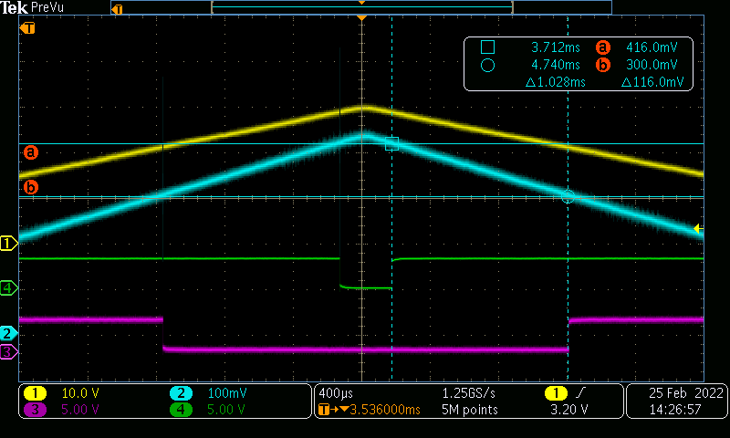
The following images show the measured output of the undervoltage and overvoltage detection circuit, comparing the AMC23C14 outputs to the VIN voltage (trace 2). These measurements confirm that the comparator trip thresholds match the desired values set by the internal comparator threshold at 300 mV, and the externally set threshold at 420 mV as defined in the equation in step 2 of the Design Steps section.
 Waveform of IN When Vsupp is Increasing
 Waveform of IN When Vsupp is Decreasing
Design Featured Device
| Device | Key Features | Device Link |
|---|---|---|
| AMC23C14 |
|
Device: AMC23C14 Similar Devices: Isolated amplifiers |
Design References
See Analog Engineer's Circuit Cookbooks for TI's comprehensive circuit library.
Texas Instruments, AMC23C14 AMC23C14 Dual, Fast Response, Reinforced Isolated Window Comparator With Adjustable Threshold data sheet