SBOA327A December 2019 – August 2021 OPA182 , OPA2182 , OPA4182 , TLV9042 , TLV9062
Design Goals
| Input | Output | Supply | |||
|---|---|---|---|---|---|
| ViMin | ViMax | IoMin | IoMax | Vcc | Vee |
| 0V | 2V | 0mA | 100mA | 5V | 0V |
Design Description
This single-supply, low-side, V-I converter delivers a well-regulated current to a load which can be connected to a voltage greater than the op-amp supply voltage. The circuit accepts an input voltage between 0V and 2V and converts it to a current between 0mA and 100mA. The current is accurately regulated by feeding back the voltage drop across a low-side current-sense resistor, R3, to the inverting input of the op amp.
Design Notes
- A device with a rail-to-rail input (RRI) or common-mode voltage that extends to GND is required.
- R1 helps isolate the amplifier from the capacitive load of the MOSFET gate.
- Feedback components R2 and C1 provide compensation to ensure stability during input or load transients, which also helps reduce noise. R2 provides a DC feedback path directly at the current setting resistor (R3) and C1 provides a high-frequency feedback path that bypasses the MOSFET.
- The input bias current will flow through R2, which will cause a DC error. Therefore, ensure that this error is minimal compared to the offset voltage of the op amp.
- Use the op amp in a linear operating region. Linear output swing is usually specified under the AOL test conditions provided in the op amp data sheet.
Design Steps
- Determine the transfer function.
- Calculate the sense resistor, R3.
- Calculate the maximum power dissipated into the sense resistor, R3, to ensure the resistor power ratings are not exceeded.
- See the Design References section, [2] for the design procedure on how to properly size the compensation components, R1, R2, and C1.
Design Simulations
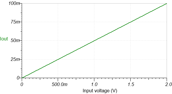
DC Simulation Results
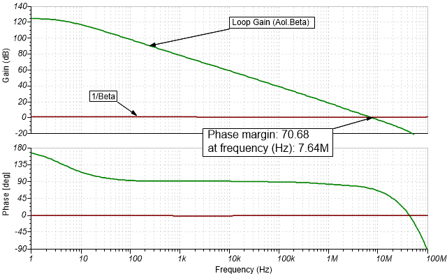
Loop Stability Simulation Results
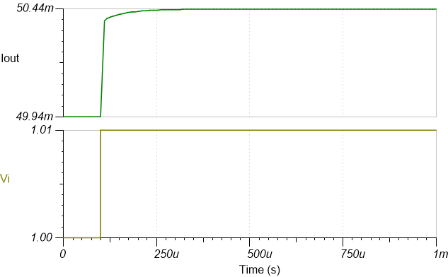
Step Response
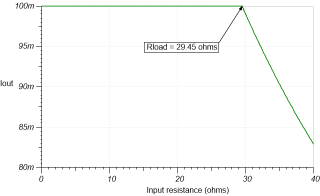
Compliance Voltage
Set output to full-scale (100 mA) and test the maximum load resistance.
Design References
- See Analog Engineer's Circuit Cookbooks for TI's comprehensive circuit library.
- TI Precision Labs
Design Featured Op Amp
| TLV9062 | |
|---|---|
| Vss | 1.8 V to 5.5 V |
| VinCM | Rail-to-rail |
| Vout | (Vcc + 60mV) to (Vee – 60mV) at RL = 2kΩ |
| Vos | 1.6mV |
| Iq | 0.538mA |
| Ib | 0.5pA |
| UGBW | 10MHz |
| SR | 6.5V/µs |
| #Channels | 1, 2, 4 |
| www.ti.com/product/TLV9062 | |
Design Alternate Op Amp
| TLV9042 |
OPA2182 |
|
|---|---|---|
| Vss | 1.2V to 5.5V |
4.5V to 36V |
| VinCM | Rail-to-rail |
(Vee – 0.1V) to (Vcc – 2.5V) |
| Vout | Rail-to-rail |
Rail-to-rail |
| Vos | ±0.6mV |
±0.45μV |
| Iq |
0.01mA |
0.85mA |
| Ib | ±1pA |
±50pA |
| UGBW | 350kHz |
5MHz |
| SR | 0.2V/µs |
10V/μS |
| #Channels |
1,2,4 |
2 |
| www.ti.com/product/TLV9042 |