SLAAE51 March 2022 MSP430FR2422 , MSP430FR2433
1 Application Brief
Introduction
This design describes how to use the MSP430FR2433 microcontroller (MCU) to build I2C communication as an I2C controller with the highly-integrated battery charge management and system power path management device BQ25890 on the BQ25890EVM-664. The BQ25890 uses an I2C-compatible interface for flexible charging parameter programming and device status reporting. The I2C communication speed is set to 100 kHz. The functionality described here is useful for devices that need to implement I2C communication with MSP430 MCUs.
I2C Communication Modes
In I2C mode, MSP430FR2433 eUSCI_B module can operate in host transmitter, host receiver, slave transmitter, or slave receiver mode. In the case described here, the MSP430FR2433 works as a host, operating in the following modes: single-byte read, single-byte write, multi-bytes read and multi-bytes write.
The I2C communication logic differs depending on the mode. For details on the basic communication protocol, refer to the BQ25890 product folder, which explains the START (S) and STOP (P) conditions, Byte Format, Acknowledge (ACK) and Not Acknowledge (NACK), Slave Address and Data Direction Bit of the transaction.
In the single-write mode (see Figure 1-1), the transaction begins with a START (S). After the START, a slave address is sent. This address is 7 bits long and is followed by the eighth bit as a data direction bit (bit R/W). A zero indicates a transmission (WRITE) and a one indicates a request for data (READ). Then an acknowledge bit is sent, which allows the receiver to signal the transmitter that the byte was successfully received and another byte may be sent. Each byte must be followed by an acknowledge bit. After the acknowledge bit, the register address is sent to specify the starting register address in the BQ25890 that the host will write. An acknowledge bit is sent again. Finally, one byte data on the SDA line is written to the BQ25890. The bus is free after the STOP condition.
Figure 1-2 shows the single-read mode. In addition to basic read and write, I2C read is multiplexed, and the transmission process has two START (S) signals. Typically, in the first transmission, the host sends data indicating the register or memory address inside the slave device after finding the slave through slave address; In the second transmission, the contents of the address are read. In other words, the first communication is to write an address to slave where the host wants to access, and the second is the actual contents of the read.
For the multi-write mode (see Figure 1-3) and multi-read mode (see Figure 1-4), the number of bytes to be transmitted in each transfer is unrestricted. The charger device supports multi-read and multi-write on REG00 (register address 0x00) through REG14 (register address 0x14) except REG0C. REG0C is a fault register. REG0C stores the fault information from last read until the host issues a new read. A Stop signal is generated when the long bytes data read or write is complete.
Implementation
This section introduces the operation of the BQ25890 on the BQ25890EVM-664 to help explain this specific implementation.
The BQ25890 is highly-integrated 5-A switch-mode battery charge management and system power path management device for single cell Li-ion and Li-polymer batteries. The BQ25890 supports high input voltage fast charging. The low-impedance power path optimizes switch-mode operation efficiency, reduces battery charging time, and extends battery life during discharging phase. For more information, refer to the BQ25890 product folder. Table 1-1 lists the I2C address of BQ25890.
| Device | 7-Bit Address | Hexadecimal (7 Bit) | Decimal (7 Bit) |
|---|---|---|---|
| BQ25890 | 01101010 | 0x6A | 106 |
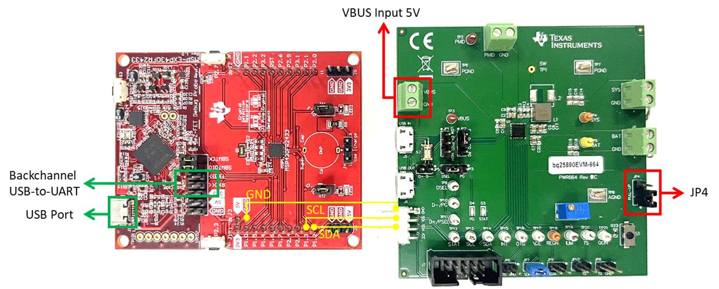
Table 1-2 lists the pin connections of the BQ25890 to the MSP430 MCU.
| Pin Function | BQ25890EVM-664 Pin | MSP-EXP430FR2433 Pin |
|---|---|---|
| I2C SCL | J8.2 | P1.3 |
| I2C SDA | J8.3 | P1.2 |
| PGND Pin | J8.1 | GND |
The hardware connection in Figure 1-5 is used in this application. First connect the MSP430FR2433 LaunchPad kit to the BQ25890EVM-664. Make sure that the BQ25890EVM-664 is in right direction by checking the SCL and SDA pinout on the two boards. Second, connect the related headers on BQ25890EVM-664, like JP1, JP2, JP3, …, JP10. For detailed description, see to the BQ25890 product folder. JP4 must be set to high level for I2C communication, because the SDA and SCL pins are open drain and must be connected to the positive supply voltage through a current source or pullup resistor.
 Figure 1-5 Hardware Connection
In this application, after a device reset, the MSP430 MCU sources the subsystem host clock (SMCLK) from the DCO configured to run at 8 MHz. The device then does the peripheral initialization. Later, the MSP430 MCU continues to send or receive data with the BQ25890. Choose the read or write mode by the host computer, and the slave address, slave register, and the length of bytes also can be configured.
To help the user understand the demo, a GUI shows the results. Figure 1-6 shows the system diagram for this implementation. The MSP430FR2433 continues to transact data with the BQ25890 and update data to the GUI through the backchannel UART.
The MSP430FR2433 LaunchPad™ development kit should be used with this example project. The backchannel UART interface on the eZ-FET is used for UART communication with the GUI. Select a baud rate of 9600 with one stop bit and no parity. The COM channel number information can be found in the PC device management under the control panel.
Performance
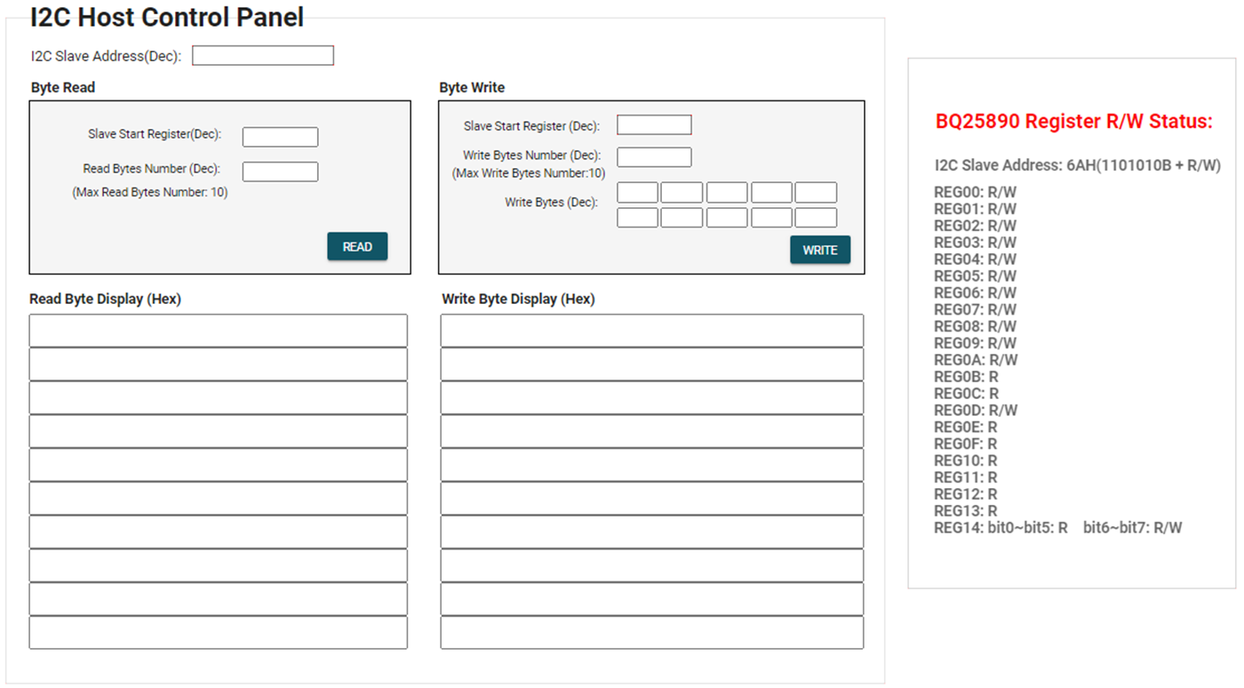
The GUI is used to input data and display the information feedback from the host controller MSP430 MCU. Figure 1-7 shows an overview of GUI. On the top of the GUI, there is one text box to enter the I2C slave address. For example, the slave address of BQ25890 is 0x6A. Below "I2C Slave Address" are two boxes to display the two different modes of "Byte Read" and "Byte Write".
In "Byte Read" mode, when using the GUI as a host, there are two text boxes to input, including "Slave Start Register" and "Read Bytes Number", which sets the start register and the number of bytes that the MSP430 MCU reads. If the read bytes value is 1, this indicates single-read mode. Any other value indicates multi-read mode, the maximum number of bytes is 10. When the "Read" button is clicked, the GUI sends a command to the MSP430 MCU to read from the BQ25890, and the GUI displays the data in the related text box.
In "Byte Write" mode, there are three text boxes to input, including "Slave Start Register", "Write Bytes Number", and "Write Bytes". If the write bytes number is 1, this indicates single-write mode. Any other value indicates multi-write mode. Next, enter the bytes that the MSP430 MCU should write to the BQ25890 in the ten small boxes. These are ordered from left to right and from first line to second line. When the "Write" button is clicked, the GUI sends a command to the MSP430 MCU to write to the BQ25890, and the GUI display the data in the related text box in order. The data must be entered in decimal format, and it is displayed in hexadecimal format in both "Byte Read" mode and "Byte Write" mode.
 Figure 1-7 I2C Communication GUI
Figure 1-8 shows a code flowchart to help with understanding of the software.
 Figure 1-8 I2C Communication Workflow
To Get Started
1. Watch our training video "MSP I2C Host with Battery Charger IC", where we walk through how to use a GUI to show I2C data.
2. Order an MSP430FR2433 LaunchPad kit and BQ25890EVM-664 for evaluation.
3. Download and test this example withMSP I2C Host with Battery Charger IC example GUI.
4. Evaluate the MSP I2C Host with Battery Charger IC example code for the MSP430FR2433 LaunchPad kit.
Device Recommendations
The device used in this example is part of the MSP430 housekeeping portfolio. This example can be used with the devices in Table 1-3 with minimal code changes.
| Part Number | Key Features |
|---|---|
| MSP430FR2433 | 16KB FRAM, 4KB SRAM, 10-bit ADC, UART/SPI/I2C, Timer |
| MSP430FR2422 | 8KB FRAM, 2KB SRAM, 10-bit ADC, UART/SPI/I2C, Timer |