SBOS694A December   2013  – November 2015 TLV3691

PRODUCTION DATA.  

  1. Features
  2. Applications
  3. Description
  4. Revision History
  5. Pin Configuration and Functions
  6. Specifications
    1. 6.1 Absolute Maximum Ratings
    2. 6.2 ESD Ratings
    3. 6.3 Recommended Operating Conditions
    4. 6.4 Thermal Information
    5. 6.5 Electrical Characteristics
    6. 6.6 Switching Characteristics
    7. 6.7 Typical Characteristics
  7. Detailed Description
    1. 7.1 Overview
    2. 7.2 Functional Block Diagram
    3. 7.3 Feature Description
    4. 7.4 Device Functional Modes
      1. 7.4.1 Nano-Power
      2. 7.4.2 Rail-to-Rail Inputs
      3. 7.4.3 Push-Pull Output
  8. Application and Implementation
    1. 8.1 Application Information
      1. 8.1.1 Comparator Inputs
      2. 8.1.2 External Hysteresis
        1. 8.1.2.1 Inverting Comparator With Hysteresis
        2. 8.1.2.2 Noninverting Comparator With Hysteresis
      3. 8.1.3 Capacitive Loads
      4. 8.1.4 Setting the Reference Voltage
    2. 8.2 Typical Application
      1. 8.2.1 Window Comparator
        1. 8.2.1.1 Design Requirements
        2. 8.2.1.2 Detailed Design Procedure
        3. 8.2.1.3 Application Curve
      2. 8.2.2 Overvoltage and Undervoltage Detection
  9. Power Supply Recommendations
  10. 10Layout
    1. 10.1 Layout Guidelines
    2. 10.2 Layout Example
  11. 11Device and Documentation Support
    1. 11.1 Device Support
      1. 11.1.1 Development Support
        1. 11.1.1.1 TINA-TI (Free Software Download)
        2. 11.1.1.2 TI Precision Designs
    2. 11.2 Documentation Support
      1. 11.2.1 Related Documentation
    3. 11.3 Community Resources
    4. 11.4 Trademarks
    5. 11.5 Electrostatic Discharge Caution
    6. 11.6 Glossary
  12. 12Mechanical, Packaging, and Orderable Information

パッケージ・オプション

メカニカル・データ(パッケージ|ピン)
サーマルパッド・メカニカル・データ
発注情報

1 Features

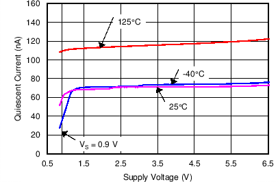
  • Low Quiescent Current: 75 nA
  • Wide Supply:
    • 0.9 V to 6.5 V
    • ±0.45 V to ±3.25 V
  • MicroPackages: DFN-6 (1 mm × 1 mm), 5-Pin SC70
  • Input Common-Mode Range Extends 100 mV Beyond Both Rails
  • Response Time: 24 µs
  • Low Input Offset Voltage: ±3 mV
  • Push-Pull Output
  • Industrial Temperature Range:
    –40°C to 125°C

2 Applications

  • Overvoltage and Undervoltage Detection
  • Window Comparators
  • Overcurrent Detection
  • Zero-Crossing Detection
  • System Monitoring:
    • Smart Phones
    • Tablets
    • Industrial Sensors
    • Portable Medical

3 Description

The TLV3691 offers a wide supply range, low quiescent current 150 nA (maximum), and rail-to-rail inputs. All of these features come in industry-standard and extremely small packages, making this device an excellent choice for low-voltage and low-power applications for portable electronics and industrial systems.

Available as a single channel, the low-power, wide supply, and temperature range makes this device flexible enough to handle almost any application from consumer to industrial. The TLV3691 is available in SC70-5 and 1-mm × 1-mm DFN-6 packages. This device is specified for operation across the expanded industrial temperature range of –40°C to 125°C.

Device Information(1)

PART NUMBER PACKAGE BODY SIZE (NOM)
TLV3691 SC70 (5) 1.25 mm × 2.00 mm
X2SON (6) 1.00 mm × 1.00 mm
  1. For all available packages, see the orderable addendum at the end of the data sheet.

Nano-Power Operation
TLV3691 C001_SBOS694.png