SBAA531 November 2021 ADS8860 , ADS8862 , ADS8881 , ADS9110 , ADS9224R
- Trademarks
- 1Introduction
-
2
Internal Topology of SAR ADC Model
- 2.1 Sample and Hold
- 2.2 Sample and Hold Timing
- 2.3 Reference Transients
- 2.4 Bandwidth Modeling
- 2.5 Noise Modeling
- 2.6 Reference Droop and Reference Noise Errors
- 2.7 Gain, Offset, and Input Leakage Modeling
- 2.8 Differential input behavior
- 2.9 ESD Protection Diodes and Parasitic Capacitance
- 2.10 Summary of Parameters
- 2.11 Summary of Model Pins
- 3Downloading and Using PSpice® Example Projects From Web
- 4Summary
2.8 Differential input behavior
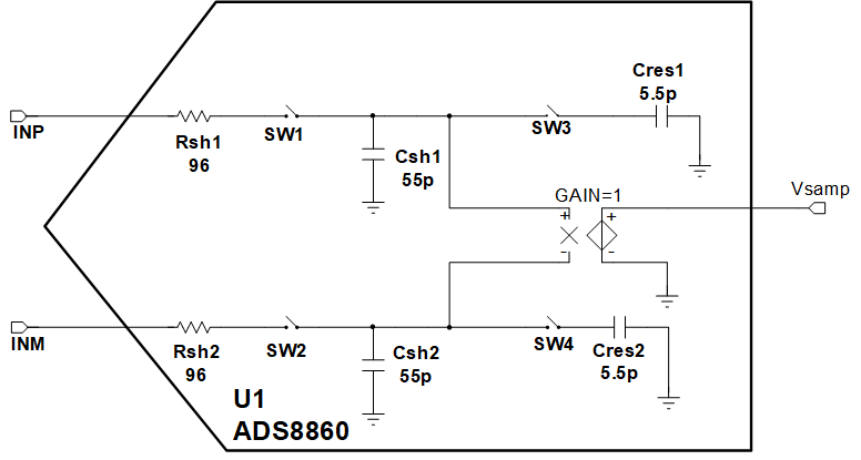
The figures shown in this application note use a single-ended configuration for simplicity. The actual model implementation uses a differential configuration. The differential configuration simply mirrors many of the key elements such as sample and hold resistors and capacitors. The output of the differential input is converted to single ended using a voltage-controlled voltage source. Figure 2-10 illustrates the differential sample and hold configuration.
 Figure 2-10 Differential Sample and
Hold