SBAA551 June 2022 ADS8661 , ADS8665 , ADS8671 , ADS8675 , ADS8681 , ADS8685 , ADS8689 , ADS8691 , ADS8695 , ADS8699 , INA823 , INA826 , LM317L , LM337L , MUX509 , TPS2661 , TPS560430
2.2 Multiplexer Stage
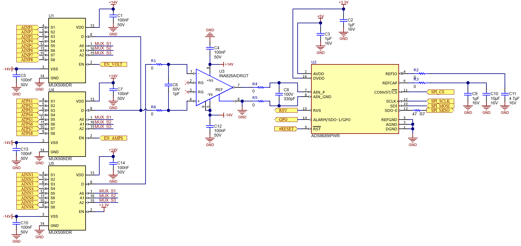
The multiplexer stage consists of three MUX508 multiplexers (see left side of Figure 2-2). Multiplexer U5 switches signal AINN of the 8 input channels, multiplexer U4 switches the shunt voltage in current mode, and multiplexer U1 selects the input voltage in voltage mode. In this design, U5 is always enabled while U1 and U4 are enabled based on the input type of the selected input channel. This design can also be implemented by other 8:1 multiplexers like TMUX6208 or TMUX7208 or by a fault-protected multiplexer like the TMUX7308F. A fault-protected multiplexer includes active shutdown circuitry in case the input signal goes beyond the supply rails. Resistors R3 and R8 can be skipped by implementing the fault-protected multiplexer in this design.
 Figure 2-2 Multiplexer, Instrumentation Amplifier and Analog-to-Digital Converter