SBAS905C November 2019 – July 2020 ADS8686S
PRODUCTION DATA
- 1 Features
- 2 Applications
- 3 Description
- 4 Revision History
- 5 Pin Configuration and Functions
-
6 Specifications
- 6.1 Absolute Maximum Ratings
- 6.2 ESD Ratings
- 6.3 Recommended Operating Conditions
- 6.4 Thermal Information
- 6.5 Electrical Characteristics
- 6.6 Timing Requirements
- 6.7 Switching Characteristics
- 6.8 Timing Diagrams: Universal
- 6.9 Timing Diagrams: Parallel Data Read
- 6.10 Timing Diagrams: Serial Data Read
- 6.11 Typical Characteristics
-
7 Detailed Description
- 7.1 Overview
- 7.2 Functional Block Diagram
- 7.3 Feature Description
- 7.4
Device Functional Modes
- 7.4.1
Device Interface: Pin Description
- 7.4.1.1 REFSEL (Input)
- 7.4.1.2 RESET (Input)
- 7.4.1.3 SEQEN (Input)
- 7.4.1.4 HW_RANGESEL[1:0] (Input)
- 7.4.1.5 SER/BYTE/PAR (Input)
- 7.4.1.6 DB[3:0] (Input/Output)
- 7.4.1.7 DB4/SER1W (Input/Output)
- 7.4.1.8 DB5/CRCEN (Input/Output)
- 7.4.1.9 DB[7:6] (Input/Output)
- 7.4.1.10 DB8 (Input/Output)
- 7.4.1.11 DB9/BYTESEL (Input/Output)
- 7.4.1.12 DB10/SDI (Input/Output)
- 7.4.1.13 DB11/SDOB (Input/Output)
- 7.4.1.14 DB12/SDOA (Input/Output)
- 7.4.1.15 DB13/OS0 (Input/Output)
- 7.4.1.16 DB14/OS1 (Input/Output)
- 7.4.1.17 DB15/OS2 (Input/Output)
- 7.4.1.18 WR/BURST (Input)
- 7.4.1.19 SCLK/RD (Input)
- 7.4.1.20 CS (Input)
- 7.4.1.21 CHSEL[2:0] (Input)
- 7.4.1.22 BUSY (Output)
- 7.4.1.23 CONVST (Input)
- 7.4.2 Device Modes of Operation
- 7.4.1
Device Interface: Pin Description
- 7.5 Programming
- 7.6 Register Maps
- 8 Application and Implementation
- 9 Power Supply Recommendations
- 10Layout
- 11Device and Documentation Support
8.2.1.2 Detailed Design Procedure
For the ADS8686S, each channel incorporates an analog front-end composed of a programmable gain amplifier (PGA), programmable analog low-pass filter (LPF), and an ADC input driver. The analog input for each channel presents a constant resistive impedance of 1 MΩ (1.2 MΩ for the 20% overrange setting) independent of the ADC sampling frequency. The high input impedance of the analog front-end circuit allows direct connection to potential transformers (PT) and current transformers (CT). The ADC inputs can support up to ±10-V, ±5-V, and ±2.5-V bipolar inputs with a 20% overrange option for each input and the integrated signal conditioning eliminates the need for external amplifiers or ADC driver circuits.
The PT and CT used in the power system, as illustrated in Figure 8-1, usually have a ±10-V or ±5-V output range. Although the PT and CT provide isolation from the power system, a series resistor (RXAP orRXBP) must be placed on the analog input channels. The series resistor helps limit the input current to ±10 mA to protect the ADC.
An LPF is usually used on each analog input channel to eliminate high-frequency noise pickup and minimize aliasing. Figure 8-2 shows a circuit example of the recommended configuration for an input RC filter. A balanced RC filter configuration matches the external source resistance on the positive path (RXAP or RXBP) with an equal resistance on the negative path (RXAM or RXBM). Matching the source impedance in the positive and negative path allows for better common-mode noise rejection and helps in maintaining the dc accuracy of the system by canceling any additional gain error contributed by the external series resistance.
 Figure 8-2 Input RC Low-Pass Filter
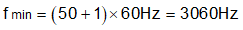
The primary goal of the data acquisition system illustrated in Figure 8-1 is to measure up to 50 harmonics in a 60-Hz power network. Thus, the analog front-end must have sufficient bandwidth, as shown in Equation 3, to detect signals up to 3060 Hz.
The pass band of the low-pass filter configuration shown in Figure 8-2 is determined by the –3-dB frequency, calculated according to Equation 4.
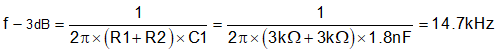
The value of C1 is selected as 1.8 nF, a standard capacitance value available in C0G type and 0603-size surface-mount components. In combination with the R1 and R2 resistors, this LPF provides sufficient bandwidth to accommodate the required 50 harmonics for the input signal of 60 Hz.