SBASA35A June 2020 – October 2020 AMC3330-Q1
PRODUCTION DATA
- 1 Features
- 2 Applications
- 3 Description
- 4 Revision History
- 5 Pin Configuration and Functions
-
6 Specifications
- 6.1 Absolute Maximum Ratings
- 6.2 ESD Ratings
- 6.3 Recommended Operating Conditions
- 6.4 Thermal Information
- 6.5 Power Ratings
- 6.6 Insulation Specifications
- 6.7 Safety-Related Certifications
- 6.8 Safety Limiting Values
- 6.9 Electrical Characteristics
- 6.10 Switching Characteristics
- 6.11 Timing Diagram
- 6.12 Insulation Characteristics Curves
- 6.13 Typical Characteristics
- 7 Detailed Description
- 8 Application and Implementation
- 9 Power Supply Recommendations
- 10Layout
- 11Device and Documentation Support
- 12Mechanical, Packaging, and Orderable Information
8.2.2.1 Input Filter Design
TI recommends placing an RC filter in front of the isolated amplifier to improve signal-to-noise performance of the signal path. Design the input filter such that:
- The cutoff frequency of the filter is at least one order of magnitude lower than the sampling frequency (20 MHz) of the internal ΔΣ modulator
- The input bias current does not generate significant voltage drop across the DC impedance of the input filter
- The impedances measured from the analog inputs are equal
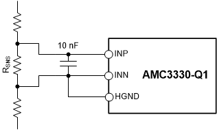
Most voltage sensing applications use high-impedance resistor dividers in front of the isolated amplifier to scale down the input voltage. In this case, a single capacitor shown in Figure 8-2 is sufficient to filter the input signal.
 Figure 8-2 Differential Input
Filter