SBAU230C August 2014 – March 2021 ADS8688
3.2 Voltage Reference, Aux Input, and Supply Decoupling
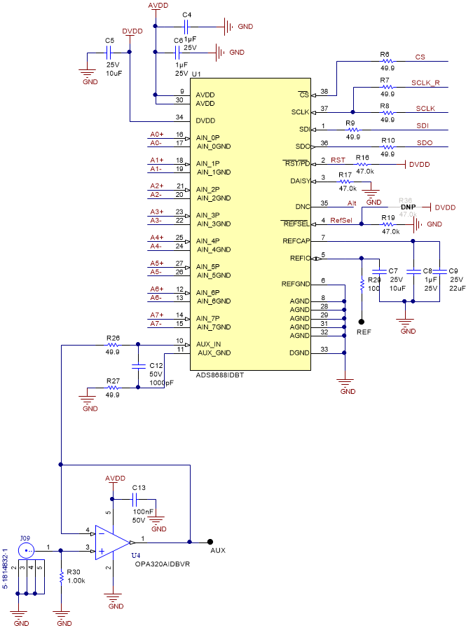
The circuit shown in Figure 3-2 illustrates the decoupling on AVDD, DVDD, and the reference IO. It is possible on the ADS8688 to use an external voltage reference, but typically the integrated internal reference is sufficient. In cases where you need to use an enthral voltage reference it can be connected via the REF test point. The capacitors for decoupling match the recomendations in the ADS8688 data sheet. The layout (see Figure 8-1) uses the shortest possible connections to the decouplign capacitors and connections the ground end to the GND plane using vias. The AUX input is a standard SAR input and does not have an analog front end. Thus, this input cannot accept high voltage input signals (Vin Full Scale = VREF = 4.096V). Furthermore, this input requires an external buffer amplifier U4 to achieve good settling.
 Figure 3-2 Voltage Reference, Aux Input, and Supply Decoupling