SBAU394B April 2022 – August 2025
2.2 ADC Connections and Decoupling
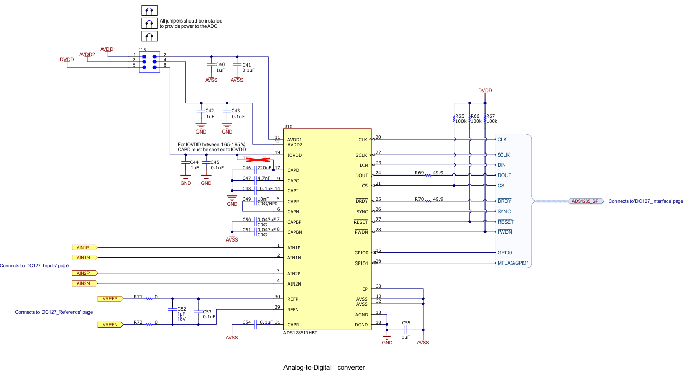
Figure 2-2 shows all connections to the ADS1285 (U10). Each power supply connection has 0.1-μF and 1-μF decoupling capacitors. Make sure these capacitors are physically close to the device and have a good connection to the respective ground plane (GND or AVSS). The supply connections pass through a set of jumpers (J15). These jumpers enable power supply current measurements by the removing the shunt and inserting an ammeter between the supply power and the ADC pin. Alternatively, remove the shunts on jumper J15 and apply an external power source directly to the corresponding supply pin if desired. For more information about the required voltage and current levels for an external supply, see the Section 2.3, Table 1-2, and the ADC data sheet.
 Figure 2-2 ADS1285 Connections and
Decoupling
Figure 2-2 ADS1285 Connections and
DecouplingBy default, the EVM IOVDD is configured for 3.3V operation. Install resistor R68 to connect IOVDD to CAPD and enable 1.8V operation. Do not use the PHI board when R68 is installed. The IOVDD absolute maximum voltage is 2.2V and the maximum operating voltage is 1.95V with R68 installed. Applying 3.3V with R68 installed causes permanent damage to the ADS1285.
Several digital pins have a 49.9Ω series resistor. These resistors smooth the edges of the digital signals to provide minimal overshoot and ringing. The CS, PWDN, and RESET pins each have a 100kΩ pull-up resistor. These resistors verify that the ADC powers up in a known state.