SBAU394B April 2022 – August 2025
5.1 Schematics
Figure 5-1 shows a block diagram of the ADS1285EVM-PDK.
 Figure 5-1 ADS1285EVM-PDK Block
Diagram
Figure 5-1 ADS1285EVM-PDK Block
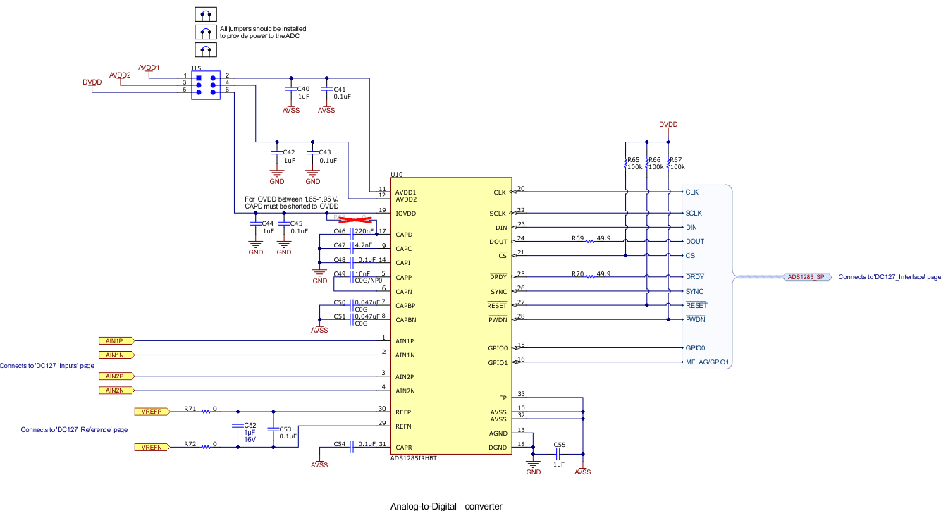
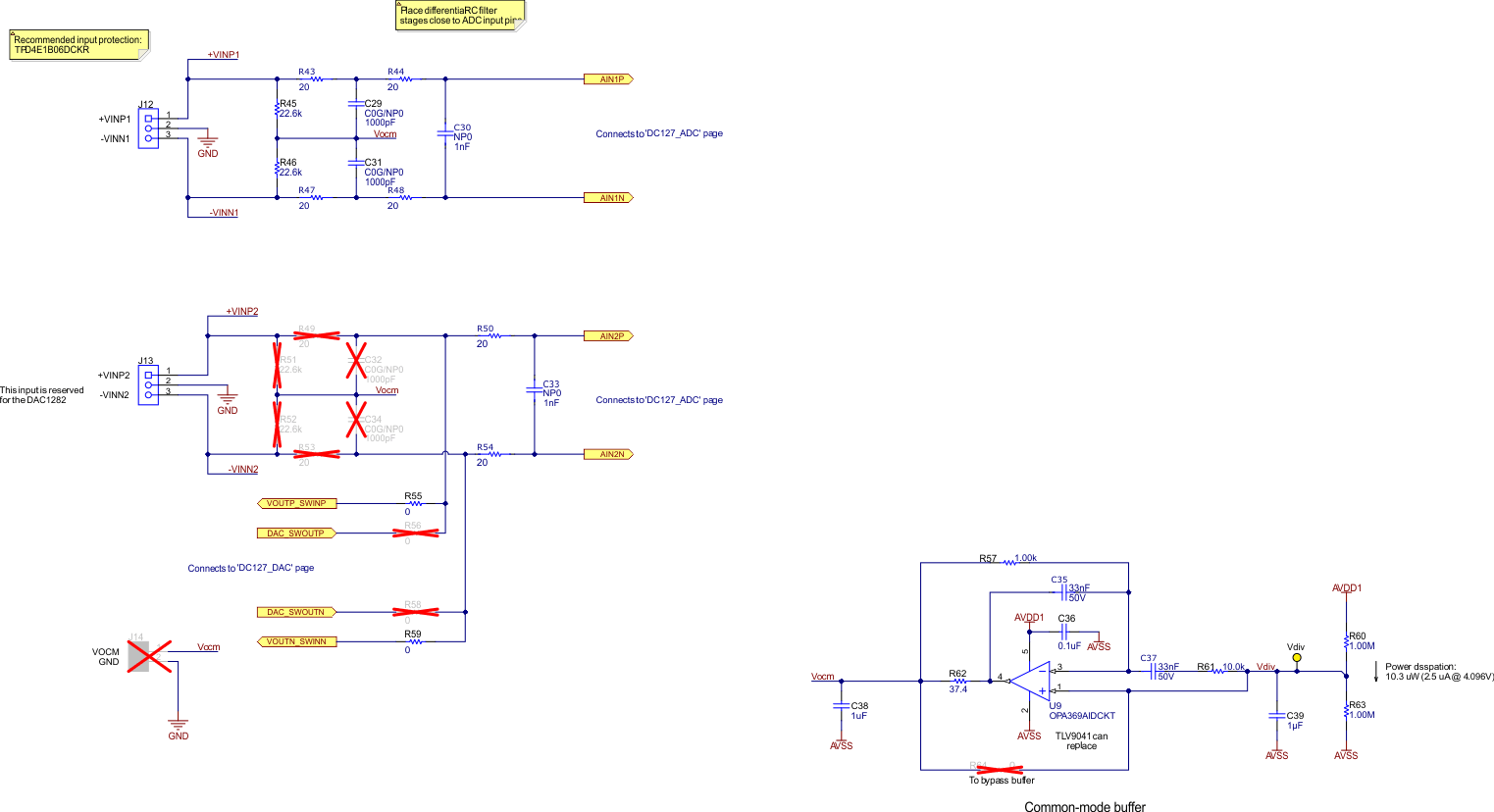
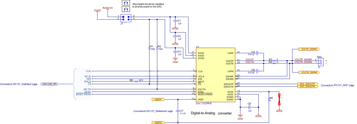
DiagramFigure 5-2 through Figure 5-7 illustrate various schematics for the ADS1285EVM-PDK ADC.
 Figure 5-2 ADS1285EVM-PDK ADC
Schematic
 Figure 5-3 ADS1285EVM-PDK Analog Inputs
and Common-Mode Buffer Schematic
 Figure 5-4 ADS1285EVM-PDK Clock and
Interface Schematic
 Figure 5-5 ADS1285EVM-PDK Power-Supply
Schematic
 Figure 5-6 ADS1285EVM-PDK Reference
Voltage Schematic
 Figure 5-7 ADS1285EVM DAC
Schematic