SBOA229 June 2021 OPA325 , TLV316 , TLV9062
| Input | Output | Supply | |||
|---|---|---|---|---|---|
| ViMin | ViMax | VoMin | VoMax | Vcc | Vee |
| –2.45V | +2.45V | 0.05V | 4.95V | 5V | 0V |
| Gain | Low Cutoff Frequency (fl) | High Cutoff Frequency (fh) | Vref |
|---|---|---|---|
| 1V/V | 1kHz | 10kHz | 2.5V |
Design Description
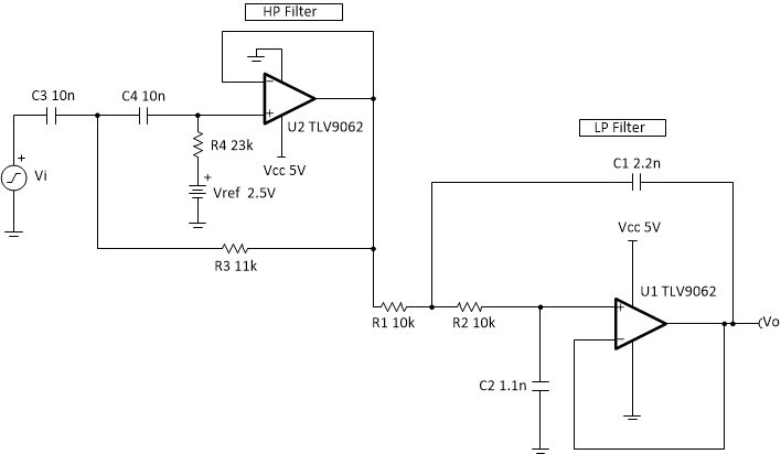
This circuit is a single-supply, 2nd-order Sallen-Key (SK) band-pass (BP) filter. It is designed by cascading an SK low-pass filter and an SK high-pass filter. Vref provides a DC offset to accommodate for a single supply.
Design Notes
- Select an op amp with sufficient input common-mode range and output voltage swing.
- Add Vref to bias the input signal to meet the input common-mode range and output voltage swing.
- Select the capacitor values first since standard capacitor values are more coarsely subdivided than the resistor values. Use high-precision, low-drift capacitor values to avoid errors in fl and fh.
- To minimize the amount of slew-induced distortion, select an op amp with sufficient slew rate (SR).
- For HP filters, the maximum frequency is set by the gain bandwidth (GBW) of the op amp. Therefore, be sure to select an op amp with sufficient GBW.
Design Steps
This BP filter design involves two cascaded filters, a low-pass (LP) filter and a high-pass (HP) filter. The lower cutoff frequency (fl) of the BP filter is 1kHz and the higher cutoff frequency (fh) is 10kHz. The design steps show an LP filter design with fh of 10kHz and an HP filter design with fl of 1kHz. See the SK LP filter design and SK HP filter design in the circuit cookbook for details on transfer function equations and calculations.
LP Filter Design
- Use SK low-pass filter design to determine R1 and R2.
- Use SK low-pass filter design to determine C1 and C2.
HP Filter Design
- Use SK high-pass filter design to determine C3 and C4.
- Use SK high-pass filter design to determine R3 and R4.
Design Simulations
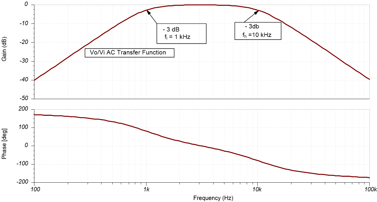
AC Simulation Results
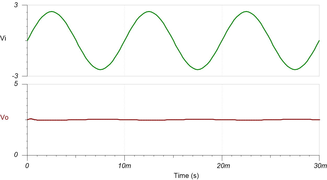
Transient Simulation Results
The following image shows a filter output in response to a 5-Vpp, 100-Hz input signal (gain = 0.01 V/V).
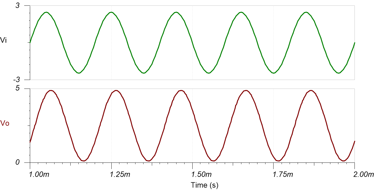
The following transient simulation result shows a filter output in response to a 5-Vpp, 5-kHz input signal
(gain = 1V/V).
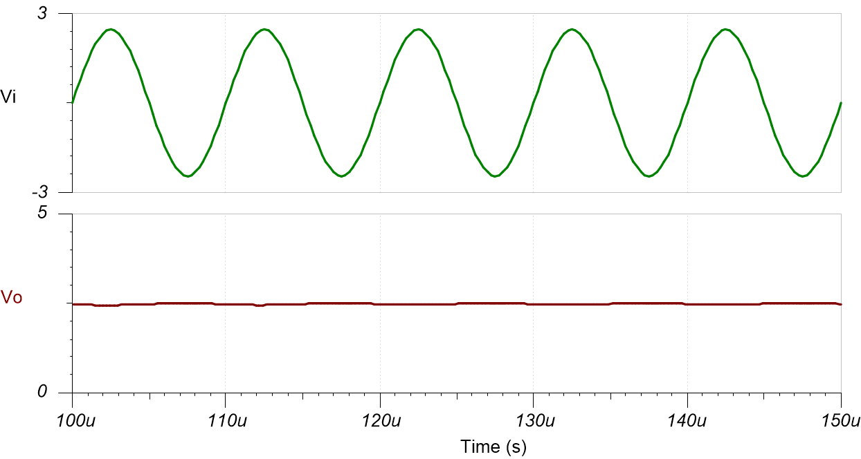
The following image shows a filter output in response to a 5-Vpp, 100-kHz input signal (gain = 0.01V/V).
Design References
- See Analog Engineer's Circuit Cookbooks for TI's comprehensive circuit library.
- TI Precision Labs.
Design Featured Op Amp
| TLV9062 | |
|---|---|
| Vss | 1.8V to 5.5V |
| VinCM | Rail-to-Rail |
| Vout | Rail-to-Rail |
| Vos | 0.3mV |
| Iq | 538µA |
| Ib | 0.5pA |
| UGBW | 10MHz |
| SR | 6.5V/µs |
| #Channels | 1, 2, 4 |
| www.ti.com/product/TLV9062 | |
Design Alternate Op Amp
| TLV316 | OPA325 | |
|---|---|---|
| Vss | 1.8V to 5.5V | 2.2V to 5.5V |
| VinCM | Rail-to-Rail | Rail-to-Rail |
| Vout | Rail-to-Rail | Rail-to-Rail |
| Vos | 0.75mV | 0.150mV |
| Iq | 400µA | 650µA |
| Ib | 10pA | 0.2pA |
| UGBW | 10MHz | 10MHz |
| SR | 6V/µs | 5V/µs |
| #Channels | 1, 2, 4 | 1, 2, 4 |
| www.ti.com/product/TLV316 | www.ti.com/product/OPA325 |