SBOA236A October 2017 – March 2022 INA125 , INA188 , INA818 , INA819 , INA821 , INA826 , TLV07 , TPS54335A
1
Introduction
Battery test equipment is used to verify battery pack functionality and performance prior to shipment to the customer. This application brief outlines three major functional tests that a battery tester performs while showing how to achieve the desired level of regulated error.
 Figure 1-1 Traditional Battery Test
 Equipment Block Diagram
Formation and Grading of Batteries
After the battery cell or battery pack is assembled, each unit must undergo at least one fully controlled charge or discharge cycle to initialize the device, and convert it to a functional power storage device. Battery vendors also use this process to grade battery cells, the process of separating the cells into different performance groups according to target specifications. For a more in-depth look at the battery initialization circuit, view our Bi-Directional Battery Initialization System Power Board Reference Design.
Loop and Feature Test
The loop and feature test refers to cycling the battery cell or battery pack through repeated charging and discharging sequences. This verifies that the battery’s characteristic life and reliability parameters to assure they are within the specified range of the defined tolerances.
Function Test
Functional testing verifies that the battery pack is operational prior to shipment to the customer. This assures that each battery cell and battery pack is working properly.
Amplifier Usage in Battery Test Equipment
In typical systems, a Buck converter is used as the power source for battery charging and a Boost converter is used for battery discharge. Both conventional operational amplifiers (Op Amps) and instrumentation amplifiers (INAs) are used in the feedback loop to control both the charging and discharging voltage and current.
To charge the battery, the buck converter is enabled while the first-stage voltage Op Amps and current-sense INA are used to measure battery voltage and charging current of the battery cell or battery pack. The switch between the current-sense Op Amp and the sense resistor s that the input to the current-sense Op Amp is positive regardless of the direction of current flow across the sense resistor. These conditioned signals serve as the input to the second stage error Op Amp for either the voltage loop or current loop, respectively.
The gained up output from each error Op Amp serves as the input to the third-stage buffer Op Amp. The output of the buffer Op Amp feeds into the feedback pin of the buck converter to control the output voltage or current. Depending on the output current requirements, the buck-boost functions can be accomplished several ways; however, two approaches are the most common.
For higher current requirements, an integrated charge controller and external FET can be used. However, for lower-current requirements, which are common in cost-sensitive systems, this function can be implemented discretely as shown in Figure 1-2. The design engineer can adjust VV_ref and VI_ref on the positive input pins of the error Op Amps to adjust the target output voltage and current of the buck converter to the optimal value.
In a typical battery charging application, the output voltage of the current-loop error Op Amp starts high, putting the buck converter into constant current output.
In the next phase, the output voltage of the voltage-loop error Op Amp goes high, putting the buck converter into constant voltage output. When the battery is being discharged, the boost converter is enabled. The Op Amps control the battery discharge current and voltage, functioning in the same manner as they do when the battery is being charged. The boost converter boosts the battery voltage to VDC, which is usually 12 V.
Typical Amplifier Configuration
System and Amplifier Requirements
Typical system requirements:
- Regulated current error ERRIout = 0.1%
- Regulated voltage error ERRVout = 0.5%
To achieve the above requirements, an Op Amp with low offset voltage (VOS), low VOS temperature drift and high CMRR, like the TLV07 is needed.
The Op Amps create a closed loop with the power stage, the voltage on the inverting input of the error Op Amp will be very close to the reference voltage VV_ref and VI_ref, thus minimizing the error from the large loop gain.
Since the major errors come from the voltage- and current-sense amplifiers, it’s important to select high precision amplifiers.
For example, if the desired regulated output current target, ISET is 10A, and the current sensing resistor, RSENSE is 20mΩ, the input error of amplifier will be:


If the desired regulated output voltage is set to VSET 4.2 V, the input error of amplifier will be:
Assuming the temperature rises from 25°C to 85°C and the battery voltage is 4 V, we can easily calculate the real world error from one of our low-offset and low offset drift Op Amps, the TLV07.
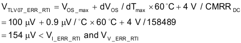
Using the calculated numbers above, it is clear that a precision Op Amp similar to TLV07 is an ideal Op Amp to meet the system output current and voltage error requirements.
For our next example, we use an INA which integrates all the feedback resistors. delivers VOS_max = 150 µV and dVOS/dTmax = 0.5 µV/°C and is a good fit to perform the current-shunt amplifier function in a system with a simplified design.
If the system requires even higher performance specifications, the current and voltage error can be changed to 0.05% and 0.1%, respectively. In this case, precision INAs such as the zero-drift INA188, can be used. Assuming the same conditions from the above example, with a 60°C temperature rise and VBAT of 4 V, the real-world error from the INA188 is: VI_ERR_RTI= 67 µV and VV_ERR_RTI< = 4.2 mV
Reference Circuit of Amplifier in Each Stage
Looking at the voltage and current sense reference circuit shown in Figure 1-3, I+ and I- contributions are resultant of the current sense resistors. The B+ and B- components are from the positive and negative terminals of the battery. Since the actual battery voltage might be higher than 5 V, the typical Op Amp power supply is 12 V. The TLV07, INA188 and INA125 all have 36 V max (±18 V) supply voltage, meeting system requirements.
As battery current can be close to zero during charge and discharge cycles, a bi-polar supply is implemented in the first stage current-sensing Op Amp to avoid clipping the current sense signal. Type-III compensation is applied on each stage of the error Op Amp , with R12, C3, C4 and R6, C1, C2 respectively. To assure loop stability, these values should be fine-tuned based on the actual power supply design.
Conclusion
Voltage and current sensing are the two most significant measurements in battery test equipment systems. Furthermore, the most important parametric characteristics for this application is a precision Op Amp or INAs that feature low voltage-offset and drift. These parameters are critical to assure high-performance sensing while minimizing the first stage contribution to system error.
Battery Test Equipment
| Device | System Benefits | |
|---|---|---|
| TLV07
(Op Amp) Device |
Low-offset voltage and low-drift provide sufficient regulated current and voltage error for cost-sensitive systems | |
| INA125 (Instrumentation amplifier) |
High CMR (common mode rejection) of (100 dB Min) increases dynamic range at the output; low offset voltage and low drift reduce the need for costly and time-consuming calibration | |
| INA188 (Instrumentation amplifier) |
Low-offset voltage and zero-drift provide lower regulated current error and voltage error while a high CMR (104 dB Min) decreases common mode interference | |