SBOA268A February 2018 – January 2019 OPA1671 , OPA170 , OPA855 , OPA858
Design Goals
| Input | Output | BW | Supply | |||
|---|---|---|---|---|---|---|
| IiMin | IiMax | VoMin | VoMax | fp | Vcc | Vee |
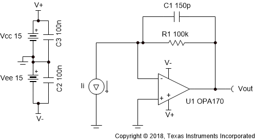
| 0 A | 50 µA | 0 V | 5 V | 10 kHz | 15 V | –15 V |
Design Description
The transimpedance op amp circuit configuration converts an input current source into an output voltage. The current to voltage gain is based on the feedback resistance. The circuit is able to maintain a constant voltage bias across the input source as the input current changes which benefits many sensors.
Design Notes
- Use a JFET or CMOS input op amp with low bias current to reduce DC errors.
- A bias voltage can be added to the non-inverting input to set the output voltage for 0 A input currents.
- Operate within the linear output voltage swing (see Aol specification) to minimize non-linearity errors.
Design Steps
- Select the gain resistor.
- Select the feedback capacitor to
meet the circuit bandwidth.
- Calculate the necessary op amp gain
bandwidth (GBW) for the circuit to be stable.
- Cs: Input source capacitance
- Cd: Differential input capacitance of the amplifier
- Ccm: Common-mode input capacitance of the inverting input
Design Simulations
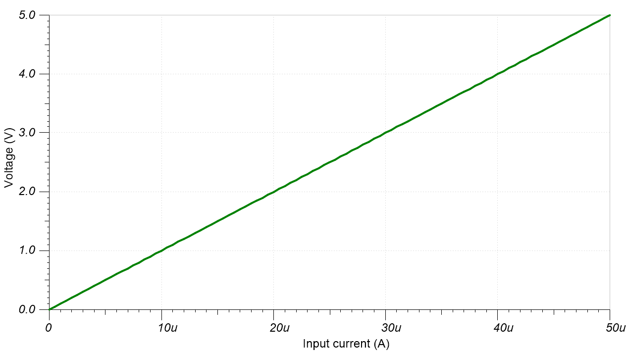
DC Simulation Results
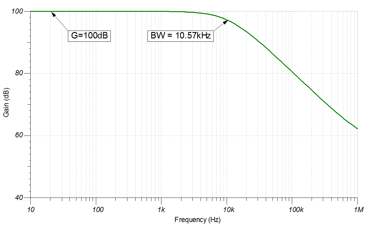
AC Simulation Results
Design References
See Analog Engineer's Circuit Cookbooks for TI's comprehensive circuit library.
See circuit SPICE simulation file SBOC501.
See TIPD176.
Design Featured Op Amp
| OPA170 | |
|---|---|
| Vcc | 2.7 V to 36 V |
| VinCM | (Vee–0.1 V) to (Vcc –2 V) |
| Vout | Rail–to–rail |
| Vos | 0.25 mV |
| Iq | 0.11 mA |
| Ib | 8 pA |
| UGBW | 1.2 MHz |
| SR | 0.4 V/µs |
| #Channels | 1, 2, and 4 |
| OPA170 | |
Design Alternate Op Amp
| OPA1671 | |
|---|---|
| Vcc | 1.7 V to 5.5 V |
| VinCM | Rail–to–rail |
| Vout | (Vee+10 mV) to (Vcc-10 mV) at 275 µA |
| Vos | 250 µV |
| Iq | 940 µA |
| Ib | 1 pA |
| UGBW | 12 MHz |
| SR | 5 V/µs |
| #Channels | 1 |
| OPA1671 | |