SBOA400 July 2020 – MONTH TMCS1100 , TMCS1100-Q1 , TMCS1101 , TMCS1101-Q1 , TMCS1107 , TMCS1107-Q1 , TMCS1108 , TMCS1108-Q1
6 Case to Junction Temperature Correlation
Through the aforementioned measurement technique, the maximum load for a cutoff junction temperature of 135°C was found for a few different PCB layouts, shown in Figure 6-1 through Figure 6-8. One layout is the TMCS1100EVM, which is optimized for large loads in a hot environment. The EVM layout has large input planes, 3 oz. copper layers, and copper layers on both the top and bottom layers of the board. The other layouts are a variation of the EVM layout with 1 or more thermal optimization attributes removed. The board names and layout variations are described in Table 6-1.
| Layout | Copper Weight | Top Copper | Bottom Copper | Large Input Load Planes |
|---|---|---|---|---|
| EVM (E1) | 3 oz. | x | x | x |
| L1 | 1 oz. | x | x | x |
| L2 | 1 oz. | x | x | |
| L3 | 1 oz. | x |
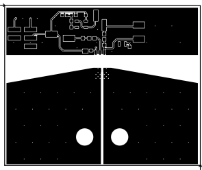 Figure 6-1 EVM (E1) Layout Top
Layer
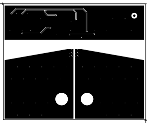 Figure 6-2 EVM (E1) Layout Bottom
Layer
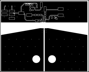 Figure 6-3 L1 Layout Top
Layer
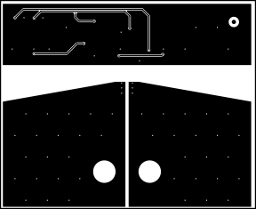 Figure 6-4 L1 Layout Bottom
Layer
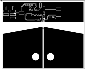 Figure 6-5 L2 Layout Top
Layer
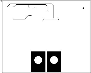 Figure 6-6 L2 Layout Bottom
Layer
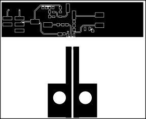 Figure 6-7 L3 Layout Top
Layer
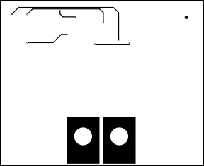 Figure 6-8 L3 Layout Bottom
Layer
Figure 6-8 L3 Layout Bottom
LayerMeasurement Results
Case and junction measurement data was collected at three different ambient temperatures: 40°C, 85°C, and 125°C. The impact of each tier of optimization for the various layouts is observed in Figure 6-9 through Figure 6-14. The plotted data shows the measured temperature with respect to load current. The thermal handling amongst the layouts improves from left to right within each plot, where the rightmost plotted line in each figure indicates the layout that has the least temperature change per current step and can handle the most current before the junction reaches 135°C. Regardless of measurement technique, the layouts ranked from most thermally robust to least are the EVM (E1), L1, L2, and L3.
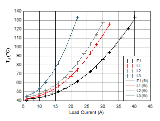 Figure 6-9 40°C Ambient Junction
Measurements
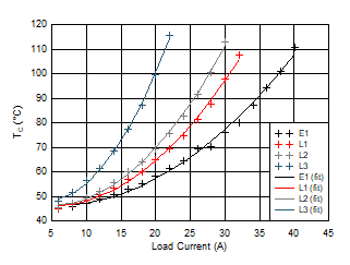 Figure 6-10 40°C Ambient Case
Measurements
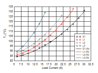 Figure 6-11 85°C Ambient Junction
Measurements
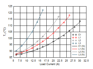 Figure 6-12 85°C Ambient Case
Measurements
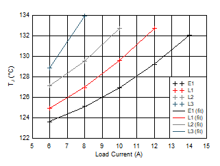 Figure 6-13 125°C Ambient Junction
Measurements
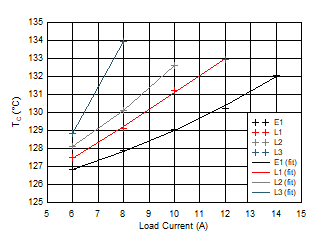 Figure 6-14 125°C Ambient Case
Measurements
Figure 6-14 125°C Ambient Case
MeasurementsKey Observations
- More copper weight (trace thickness) and wider traces sink more heat and allow larger current loads.
- Higher ambient temperature reduces maximum acceptable load.
- The load current-to-temperature relationship is non-linear (multi-order polynomial), and if measurements are done properly should exhibit a trend that can be curve fitted.
- Junction temperature does not equal case temperature.
Correlating Case to Junction
When validating a system there may not be the option to take a junction measurement, as that would require the TMCS1100 to be powered off and its ground to be isolated from the system ground in order to bias one of the diodes. Consequently, a case measurement may be preferred. This is possible provided that at least a few prior junction measurements are taken to determine the case-to-junction relationship. If using a thermocouple for case measurement as in this application report, attention to the details listed in the beginning of this application report will determine the relationship between case and junction. Overlooking these details may lead to inconsistent case measurements that are further from the junction temperature.
The previous figures indicate that the measured temperature relationship to current is non-linear and different per layout and given ambient temperature. They also show that case and junction temperature measurements exhibit different relationships to load current given the same load and ambient temperature. Despite these inconveniences, there still is a convenient relationship between junction temperature and case temperature. By plotting junction temperature versus case temperature with the ambient offset removed (TJ – TA versus TC – TA), a relatively linear relationship can be observed as shown in Figure 6-15. By removing the ambient temperature offset, the data for all layouts over all temperatures converge onto roughly the same origin with the same general trend. To determine the line that describes the trend, a least sum squares approximation can be done on all of the datapoints or on the trend lines of each layout and temperature dataset. The results for each approximation method will be different, but the deviation between methods for the presented data is within 3°C.
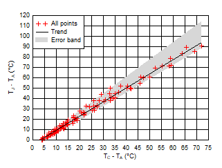 Figure 6-15 TJ – TA
vs TC – TA
Figure 6-15 TJ – TA
vs TC – TAEquation 3 provides the best approximation of all datapoints:
Using this equation, the junction temperature can now be determined based upon a case measurement and an ambient temperature (preferably taken near the device case). For instance, if the ambient temperature is 76°C and the load is 18.4A, the approximated junction temperature can be calculated as follows:
- Take the case measurement, 90.47°C.
- Subtract ambient measurement (76°C) from case measurement (90.47 °C) to get TC – TA = 14.47 °C.
- Substitute the remainder (14.47°C) into Equation 3 to get TJ – TA = 16.16°C.
- Add the ambient temperature to the solution to get the junction temperature of TJ = 92.16°C.
According to a bench test check, junction temperature was measured to be 93.16°C, thereby making the calculation only 1°C off from the measurement.
One important caveat to emphasize is the previous formula holds across multiple layouts and multiple ambient temperatures so long as the probe is precisely placed on the case. However, if a heat sink is placed on the case, thereby displacing the case probe to a trough in the heat sink, the relationship is expected to change quite dramatically. This can be observed in Figure 6-16.
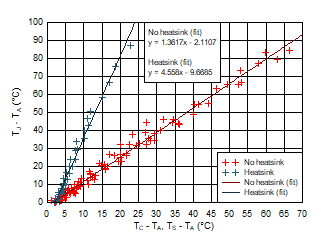 Figure 6-16 Heat Sink vs No Heat
Sink
Figure 6-16 Heat Sink vs No Heat
SinkApproximating Maximum Load
Through correlating case to junction, it is also possible to extrapolate the maximum load the device can handle for a given layout at a given ambient temperature. If sufficient case measurement points are taken and converted into junction temperature points, a curve can be fitted to predict at what load the device may fail. For instance, the case measurement data for the EVM at 40°C found in Figure 6-10 can be used to generate junction calculations with respect to load. Based off the 40°C case measurements, TJ (calc.) in Figure 6-17 was generated along with a second-order polynomial best fit equation. Through such an equation, a maximum load where TJ equals 150°C can be estimated. For this example, the maximum load based off case measurements and the corresponding junction calculations is 45 A, while the max load based off of measured junction data is estimated to be around 43.5 A. The estimate based on calculations is therefore 3.5% higher than the estimate based upon junction measurements. With more data points we expect that the percent error would decrease.
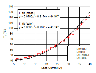 Figure 6-17 Calculated vs Measured TJ