SBOA401A June 2020 – March 2022 TMCS1100 , TMCS1100-Q1 , TMCS1101 , TMCS1101-Q1 , TMCS1107 , TMCS1107-Q1 , TMCS1108 , TMCS1108-Q1
2 Enabling Broad Electrification
Electrification enables improvements in performance, reliability, and total lifetime cost, but these systems require isolation from their high-voltage AC or DC domains in increasingly dense form factors. Many existing isolated current-sensing solutions take up significant space on high-voltage PCB designs due to additional external components, housings or elements. Hall-effect current sensors provide a monolithic, single-chip solution incorporating both the isolation and sensing elements in surface-mount form factors, such as 8-pin small-outline integrated circuit (SOIC) packages with 5 mm by 6 mm of PCB space.
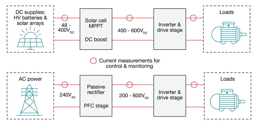
However, most sensors in 8-pin SOIC packages only provide around 400 V of a working lifetime isolation voltage, which limits the usability of these devices to systems operating below this level. For example, many high-power battery systems have 400-V nominal DC buses, and they can significantly exceed this level with load and switching transients. Industrial systems that operate from 240 VAC and convert power to a 340-VDC rectified voltage level will often include a boost stage, as Figure 2-1 shows, which can reach voltage levels of 400 VDC–600 VDC. Many solar string inverters operate with photovoltaic cell and maximum power-point tracker (MPPT) buses in the 480-V to 600-V range, which are also outside the capabilities of most available 8-pin SOIC Hall-effect current sensors.
 Figure 2-1 AC-Rectified System Including Boost
Circuit and String Inverter Circuit With MPPT Boost.
 To provide a sufficient lifetime isolation margin, the TMCS1100 and TMCS1101 devices provide 600 V of working voltage in an 8-pin SOIC form factor, with a higher lifetime margin than what is required by industry standards such as Verband der Elektrotechnik 0884-11 and Underwriters Laboratories 1577. This working voltage provides a sufficient isolation margin for equipment manufacturers without the need to transition to a larger solution size.
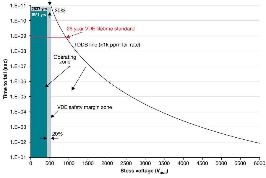
It is possible to extrapolate the expected lifetimes of a device from a qualification test known as time-dependent dielectric breakdown (TDDB), which measures the expected lifetime of a device versus the device voltage stress. Figure 2-2 shows the TMCS1100 family TDDB curve. The operating lifetime zone greatly exceeds industry standards for a 26-year lifetime with a 20% voltage safety margin.
 Figure 2-2 TDDB Curve of the TMCS1100
Family.