SBOA434 December 2020 LME49724 , OPA1632 , OPA1637 , OPA202 , OPA2202 , OPA4202 , THP210 , TLV320ADC5140
2 Super-Beta BJT
The differentiating feature of OPA1637 from the prior generation is the bipolar junction transistor (BJT) of the long-tail pair in the input circuit. This technology is called super-beta BJT. TI’s super-beta BJT is just a single BJT with high beta, that is, high current gain (Hfe).
The performance advantage of the OPA1637 comes from improvements in manufacturing technology. Precise manufacturing allows for its simple construction to achieve low noise and high frequency response with high current gain. This analog process technology improvement enables TI to design new op-amps that achieve both high DC and AC performance in bipolar op-amps. For example, BJT-input op-amps have higher input impedance with lower noise, higher bandwidth, and lower power than prior generations of transistors. While not quite as high input impedance as JFET-input op-amps, these op-amps can achieve high bandwidth while maintaining good DC precision.
This benefit is evident in not only the OPA1637 but also in other op-amps utilizing super-beta transistor technology such as the OPA2202, OPA2210, INA818, and INA819.
There are several benefits of the super-beta BJT in the input circuit of the op-amps.
 Figure 2-1 BJT small signal model
Figure 2-1 shows the small signal model of the BJT. The equation for its current gain is IB = IC/β.
This simple equation illustrates that the higher the beta, the lower the base current for a given collector current. When this transistor is part of the input differential pair of an op-amp, it amounts to a reduction of the input bias current for the op-amps. In addition, the super-beta can improve the input referred noise of the input long tail pair of op-amps with the expected and configured base current, IB, as shown in the following calculations Equation 1, Equation 2, and Equation 4.
In the BJT small signal model, the input referred noise is also modeled. The input referred voltage noise, EN, and the input referred current noise, IN, in broadband range are represented with the parameters in the BJT small signal model.
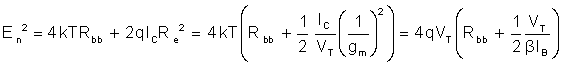

Where k is the Boltzmann constant as shown in the thermal voltage equation:
- VT is thermal voltage
- k is the Boltzmann constant
- T is temperature
- q is elementary charge
In conclusion, both the input referred voltage and current noise is kept low with the super-beta transistor.