SBOA444 November 2020 TMCS1100
4.1.5 ADC Setup
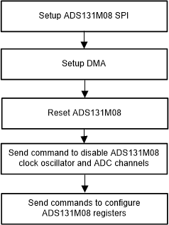
The ADC Initialization and Synchronization Process figure shows the process used to initialize the ADS131M08 before conversions are started.
 Figure 4-1 ADC Initialization and
Synchronization Process .
Next, the ADS131M08 is reset to get the device in a known state. After resetting the device, a command is sent to the ADS131M08 to disable its internal oscillator and disable the conversions on its ADC channels. Disabling the clock oscillator prevents the ADS131M08 from generating new samples when configuring the ADS131M08 registers.
Finally, commands are sent to the ADS131M08 to initialize its registers for the following configuration:
MODE register settings: 16-bit CCITT CRC used, 24-bit length for each word in the ADS131M08 packet, DRDY signal asserted on most lagging enabled channel, DRDY asserted high when conversion value is not available, DRDY asserted low when conversion values are ready
GAIN1 and GAIN2 register settings: PGA gain of 1 used for all eight ADC channels (please note that only 4 of these 8 channels are used)
CFG register settings: Current detection mode disabled
CHx_CNG register settings (where x is the channel number): All eight ADC channel inputs connected to external ADC pins and channel phase delay set to 0 for each channel (note that software phase compensation is used instead of ADS131M08 hardware phase compensation)
CLOCK register settings: 512 OSR, all channels enabled, crystal oscillator disabled, internal reference used for conversions, and high-resolution modulator power mode
At this point, the ADS131M08 is still not sampling because the crystal oscillator is still disabled. ADS131M08 sampling is not started until the rest of the setup routines of the MCU are executed. After executing these other setup routines, the MSP432 is configured to generate a port interrupt whenever a falling edge occurs on the DRDY pin, which would indicate that the ADS131M08 has new current samples that are available. Next, a command is sent to enable the crystal oscillator, which starts the voltage and current sampling.
The ADS131M08 modulator clock is derived from the crystal connected between its XTAL1 and XTAL2 pins. This clock is internally divided by two to generate the ADS131M08 modulator clock. The sampling frequency of the ADS131M08 is therefore defined as fs = fM / OSR = fADS13M08_crystal / (2 × OSR), where fs is the sampling rate, fM is the modulator clock frequency, fADS13M08_crystal is the frequency of the crystal connected to the ADS131M08, and OSR is the selected oversampling ratio. In this design, the crystal connected to the ADS131M08 has a frequency of 8.000 MHz and the oversampling ratio is selected to be 512. As a result, the ADS131M08 modulator clock is set to 4.000 MHz and the sample rate is set to 7812.5 samples per second.
In this design, the following ADS131M08 channel mappings are used in software:
AIN0P and AIN0N ADS131M08 ADC channel pins → Voltage V1 (Line-to-Neutral Voltage)
AIN5P and AIN5N ADS131M08 ADC channel pins → Current I1 (Channel A Current)
AIN4P and AIN4N ADS131M08 ADC channel pins → Current I2 (Channel B Current)
AIN3P and AIN3N ADS131M08 ADC channel pins → Current I3 (Channel C Current)