SBOA444 November 2020 TMCS1100
3.1.2 Current Measurement Analog Front End
The analog front end for current inputs is different from the analog front end for the voltage inputs. In this implementation, a TMCS1100 device is used for sensing each load current (3 devices in total). The A1 variant of the TMCS1100 is used, which has a sensitivity of 50 mV/A and allows sensing 20-A currents. The TMCS1100 Current-Sensing Circuit figure shows the TMCS1100 circuit used in this design.
 Figure 3-2 TMCS1100 Current-Sensing
Circuit.
Figure 3-2 TMCS1100 Current-Sensing
Circuit.
When designing the front-end for the TMCS1100, the voltage between the power (pin VS) and GND pins of the device must meet the following constraint:
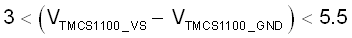
In Equation 2, VTMCS1100_VS is the voltage applied to the VS pin of the TMCS1100 device and VTMCS1100_GND is the voltage applied to the GND pin of the TMCS1100.
In this design, 5 V is selected for the voltage between VTMCS1100_VS and VTMCS110_GND, which meets the previously-listed criteria and also allows a wider current measurement range capability. Using this 5-V supply can lead to an output voltage that is larger than the input voltage range of the ADS131M08 ADCs. As a result, a voltage divider is needed to divide down the TMCS1100 output voltage to fall within the range of the ADC input range of the ADS131M08 device. R6 and R10 in the TMCS1100 Current-Sensing Circuit figure are selected to divide down the output voltage of the TMCS1100 to fit within the input ADC range of the ADS131M08 device. The R6 and R10 voltage divider results in the following input voltage at the ADC of the ADS131M08:
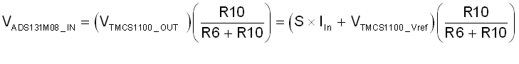
where,
VTMCS1100_OUT is the output voltage from the OUT pin of the TMCS1100 device
S is the ideal sensitivity of the device (50 mV/A in this case)
IIN is the isolated input current provided to the inputs of the TMCS1100
VTMCS1100_Vref is the voltage at the VREF pin of the TMCS1100 device
The voltage range of the ADS131M08 is calculated by subtracting the minimum voltage the ADC can sense, VADS131M08_IN,min, from the maximum voltage the ADC can sense, VADS131M08_IN,max. Since the ADS131M08 has a ±1.2-V input voltage range when using a PGA gain of 1, VADS131M08_IN,max = 1.2 V, and VADS131M08_IN,min = –1.2 V. Therefore, the input voltage range of the ADS131M08 is 2.4 V.
The values of R6 and R10 should be selected so that the maximum output voltage range from the TMCS1100 fits within the input voltage range of the ADC of the ADS131M08.
The voltage across the OUT and GND pin of the TMCS1100 device will always be less than the voltage difference across its VS and GND pin. Due to this, a conservative set of resistor values for dividing down the voltage can be calculated using the following formula:
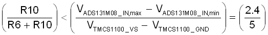
In this design, R6 was selected to be 549 Ω and R10 was selected to be 487 Ω; however, there are multiple options that can be selected for the total resistance value (R6 + R10) that would still meet Equation 4. Small values for this total resistance would increase the current drawn from the VOUT pin of the TMCS1100 device, which could limit the output voltage range of the TMCS1100. Conversely, large values for this series resistance could affect the anti-alias filter of the ADS131M08 device. In this design, the total resistance is around 1 kΩ , which does not reduce the output voltage range of the TMCS1100 and still does not significantly impact the anti-alias filter circuit for the ADS131M08.
Since the output voltage of the TMCS1100 is above 0 while half of the range of the ADS131M08 is below 0, a mechanism is needed to also level shift the voltage from the TMCS1100. This level shifting is done in this implementation by applying specific voltages to the VREF, VS, and GND pins of the TMCS1100 device.
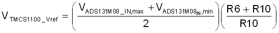
The VREF pin on the TMCS1100 is used to set the voltage output of the TMCS1100 when applying 0 A. Setting VREF to the middle of the output swing range provides bidirectional measurement capability to sense both positive and negative currents. Therefore, Vref should ideally be set to the middle of the output voltage range of the TMCS1100, as expressed in the following equation:
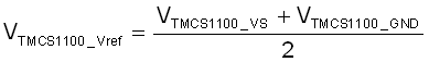
To reduce DC offset in the current readings, the zero current condition should also provide an input voltage to the ADS131M08 that is at the mid-voltage point. As a result, the value of Vref should also ideally be close to meeting the following condition:
Given that the voltage difference between the TMCS1100 Vs and GND pins is selected to be 5 V (VTMCS1100_VS – VTMCS1100_GND = 5), the two equations above can be solved to find the appropriate voltages that can be applied (with respect to the GND of the ADS131M08) on the TMCS1100 GND (VTMCS1100_GND), VS(VTMCS1100_VS), and VREF (VTMCS1100_VREF) pins. For this design, the following voltages are used to meet this criteria:
VTMCS1100_GND = –2.5 V
VTMCS1100_Vref = –0 V
VTMCS1100_VS = 2.5 V
The 2.5 V and –2.5-V voltages are created by the LM27762 in the circuit shown in the TMCS1100 GND and VS Voltage Generation Circuit figure:
 Figure 3-3 TMCS1100 GND and VS Voltage
Generation Circuit.
Figure 3-3 TMCS1100 GND and VS Voltage
Generation Circuit.
 Figure 3-4 ADS131M08 Interface Circuit
for Current Channels
Figure 3-4 ADS131M08 Interface Circuit
for Current ChannelsThe circuit in the ADS131M08 Interface Circuit for Current Channels figure consists of footprints for electromagnetic interference filter beads (R18 and R31), footprints (U5 and U7) that can be replaced with the TVS0500 for supplemental protection from surges, and an RC low-pass filter (R21, R34, and C19) that functions as an anti-alias filter. For the anti-alias filter, it should be noted that the R6 and R10 resistor values in the TMCS1100 Current-Sensing Circuit figure can affect the cutoff frequency of the anti-alias if the R6 and R10 total resistance is large; however, for the R6 and R10 resistance values used in this design, these resistor values do not significantly affect the cutoff frequency of the anti-alias filter.
To interface the differential inputs of the ADS131M08 with the single-ended output of the TMCS1100, the TMCS1100 divided output is connected to the positive terminal of the ADC channel of an ADS131M08 and the negative terminal of that ADS131M08 ADC channel is connected to the ground of the ADC. This results in the voltage at the positive terminal of the ADC swinging both above and below 0 while the voltage at the negative terminal of the ADC being fixed to the ADC GND voltage. Since the negative terminal of the ADC of the ADS131M08 is grounded, the input differential voltage to the ADC is also equal to the voltage at the positive terminal of the ADC. The VADS131M08_IN Voltage Range figure shows the voltage range of VADS131M08_IN and how this range compares to the VTMCS1100_OUT range, the VTMCS1100_VS voltage, and the VTMCS1100_GND voltage.
 Figure 3-5 VADS131M08_IN Voltage Range.