SBOA444 November 2020 TMCS1100
3.1.1 Voltage Measurement Analog Front End
The nominal voltage from the mains is from 100 V–240 V, so it needs to be scaled down to be sensed by an ADC. Since the ADS131M08 device can sense voltages down to 1.2 V, AC signals from mains can be divided down with a voltage divider and then fed to the ADS131M08 without the need for level shifters. In the board used for testing, there are four voltage sensing circuits; however, only the voltage divider circuit in the Analog Front End for Voltage Inputs figure is used for the PDU configuration referenced in this application note. The other three voltage sensing circuits are outside the scope of the PDU configuration referenced in this application note.
 Figure 3-1 Analog Front End for Voltage
Inputs.
Figure 3-1 Analog Front End for Voltage
Inputs.
At lower currents, voltage-to-current crosstalk affects active energy accuracy much more than voltage accuracy if power offset calibration is not performed. To maximize the accuracy at these lower currents, the entire ADC range is not used for voltage channels. Since the ADCs of the ADS131M08 device are high-accuracy ADCs, using the reduced ADC range for the voltage channels in this design still provides more than enough accuracy for measuring voltage. Equation 1 shows how to calculate the range of differential voltages fed to the voltage ADC channel for a given Mains voltage and selected voltage divider resistor values:
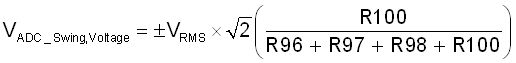
Based on this formula and the previously-stated selected resistor values, for a mains voltage of 230 V, the input signal to the voltage ADC has a voltage swing of ±246 mV (174 mVRMS). The ±246-mV voltage range is well within the ±1.2-V input voltage that can be sensed by the ADS131M08 device for the selected PGA gain value of 1 that is used for the voltage channels.