SBOA632 July 2025 DAC61401 , DAC61402 , DAC61404 , DAC714 , DAC7716 , DAC7731 , DAC7734 , DAC7744 , DAC7760 , DAC81401 , DAC81402 , DAC81404 , DAC8234 , DAC8734 , DAC8760 , DAC8771 , DAC8775 , OPA206 , OPA2206 , OPA4206 , TVS3301
Design Objective
| Key Input Parameter | Key Output Signal | Recommended Devices |
|---|---|---|
| SPI or I2C
communication to control DAC voltage output |
±10V output DAC
signal with overvoltage protection |
DAC8760, OPA206,
TPS26611, TVS3301 (optional) |
Objective: Protection of a ±10V output signal from a sustained ±32V overvoltage connection for a digital-to-analog converter (DAC) with an output buffer with a feedback sense pin.
Design Description
This circuit design describes an overvoltage protection circuit for a precision DAC output. This circuit protects the DAC output from a continuous overvoltage above the maximum and below the minimum supply voltages. In a device with a positive sense pin, the DAC output buffer is contained within the device, with a pin access to the positive sense feedback pin of the output buffer. The overvoltage protection circuit consists of an op amp with input protection set up in unity gain for the output buffer feedback sense pin, an eFuse to protect the output, and an optional transient-voltage-suppression (TVS) diode. For a DAC operating on ±15V, the output is protected to ±32V or greater without damaging the DAC and the protection circuit. This type of protective circuit buffer can be used in many industrial factory automation and control applications. This circuit is particularly useful if the output experiences an overvoltage event from miswiring at an output terminal such as in a Programmable Logic Controller (PLC).

Design Notes
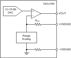
- This design protects the output of a DAC with a positive
sense pin as feedback from a sustained overvoltage event. The positive sense pin
is the feedback to output buffer of the voltage DAC. The following figure shows
the basic diagram. This sense pin is used as a Kelvin connection to provide better accuracy where there are long traces or cables. There are many DACs that are configured with the positive sense pin, but this circuit uses the DAC8760 as an example. The DAC output is set to a range of ±10V.
- If the DAC does not have a positive sense pin as feedback, the circuit in Output Overvoltage Protection Circuit for Voltage DACs Without an External Feedback Pin can be used to protect the DAC output.
- The DAC8760 has three separate power supply inputs (AVDD, VDD, and AVSS). The DAC8760 data sheet recommends using a decoupling capacitor for each power supply pin. In this circuit, parallel 100nF and 100pF capacitors are used as the decoupling capacitors for AVDD and AVSS. The DVDD pin uses a 100nF capacitor that is not shown in the circuit.
- REFOUT is the output of the DAC8760 internal reference. Connect a 100nF capacitor from the REFOUT pin to ground if the internal reference is used. REFOUT is also not shown in the circuit.
- The DAC is protected from overvoltage events using an op amp configured as a unity gain buffer to the feedback of the +VSENSE of the DAC output voltage. The output protection requires protecting the op amp input from a sustained overvoltage beyond the supply and from protecting the DAC output from sourcing or sinking excessive currents during these events.
- An optional 1kΩ resistor is placed between VOUT and +VSENSE. This resistor prevents the output buffer feedback loop of the DAC from breaking in case the feedback sense signal is cut.
- In this circuit, the OPA206 is selected for the op-amp feedback buffer used for
overvoltage protection. This op amp is selected for several characteristics:
- The offset voltage is very low and the buffer contributes little error to the DAC sense feedback. The OPA206 offset voltage is typically ±4µV (at 25°C) and ±55µV (from –40°C to 125°C).
- The OPA206 has an integrated input overvoltage
protection that extends up to ±40V beyond the op-amp supply voltage. The
input bias current relative to the input common-mode voltage for the
OPA206 is shown in the following figure.

- If an alternate op amp without integrated input overvoltage protection is used, series resistance for the inputs can be used for protection to limit the input current. For more information about overvoltage and electrical overstress in op amps, see the TI Precision Labs – Op Amps video on Electrical Overstress.
- The TPS26611 is a
current loop protector that acts as an eFuse to limit the current of the DAC8760
voltage output at the VOUT pin. The TPS26611 has a fixed bipolar current limit
of 32mA (IOL).
- In normal operation, the TPS26611 passes the DAC8760 output current. Even if the short-circuit current limit of the DAC8760 is typically 30mA, the current through the ESD diodes to the output is not limited as the output voltage is forced beyond the DAC supply voltage.
- The maximum series resistance of the TPS26611 is 12.5Ω. With an additional series resistance of 49.9Ω, the extra headroom needed at the supply output is 0.936V at an output of 15mA. With supplies of ±15V and a DAC output range of ±10V, there is plenty of headroom for DAC operation.
- The EN and SGOOD pins can be left floating.
- The MODE pin is set to ground. In this setting, the
device behavior depends on the IOUT current through the
TPS26611.
- If IOUT < IOL, then the current IOUT is passed through the TPS26611.
- If IOUT > IOL, then IOUT is quickly limited to IOL through the TPS26611 for an expiry period of 100ms (tOL_Expiry). If the current remains above IOL, the device shuts off the output and the device retries the output after a period 800ms (tRetry1).
- Current protection in the TPS26611 is bidirectional, and negative current limits in a similar manner.
- If the output voltage is forced beyond the positive or negative supply, the TPS26611 cuts off the output, preventing any damage.
- For more information about using the TPS26611 as protection for an analog output module, see the Protection for HART I/O in Analog Input and Output Modules with TPS2661x application note.
- An optional TVS diode is applied to the circuit for additional surge protection. If a TVS diode is used, the chosen breakdown voltage must be higher than any sustained overvoltage. If the breakdown voltage is less than the sustained overvoltage, then the overvoltage can damage the TVS diode. In this circuit, the expected sustained overvoltage is ±32V and an optional TVS3301 device with a bidirectional 33V breakdown is used for surge protection.
Simulation
The overvoltage protection feedback buffer is simulated with PSpice®. First, the transfer function of the buffer is simulated using a pulse voltage source as the DAC. The input of the feedback buffer is ramped from –10V to +10V, showing the full output range of the DAC. Another OPA206 is used as a model for the DAC output buffer. The OPA206 has a current limit of 25mA, which is an approximation for the DAC8760. The current limit is needed in a later simulation.

The op amp and resistor network on the left side of the figure represent the voltage DAC output and feedback. The nodes labeled +VSENSE and VOUT are pins for the DAC8760.
The transfer function from input to output of the buffer is derived from the transient simulation.

A second transient simulation shows the current during an overvoltage event.

The DAC is set to 0V and a voltage supply is placed at the output of the buffer to simulate an overstress event caused by a wiring error. The supply ramp simulates the overvoltage transition from –32V to +32V.
The simulation begins with the output at –32V, the TPS26611 eFuse is open, preventing any current from being sourced from the output of the DAC8760. The residual current at the output comes from the input of the OPA206 which has an integrated input protection, limiting the current to about 5mA. The current seen at the output of the buffer remains at 5mA as the voltage is reduced.

As the voltage increases to near the lower supply voltage of –15V, the TPS26611 begins to conduct current from the DAC output. The DAC, driven by the ramping voltage, immediately reaches the device short-circuit current limit near 30mA. This current limit is lower than the 32mA current limit level of the TPS26611, which passes the conducted current. Sustained operation of the DAC8760 current limit is not destructive.
As the ramped voltage rises above 0V, the output of the DAC changes from sourcing current to sinking current. The DAC is forced into a current limit in the opposite direction.
Finally, the ramped voltage rises above the positive supply. Because of the added voltage from the series resistance and output current, the eFuse detects the output is beyond the supply after the ramped voltage rises above +16V. After the overvoltage is detected, the TPS26611 eFuse opens again and the DAC output stops sinking current. At the output, the only remaining output current comes from the OPA206 input overvoltage protection.
A similar simulation is run to show the voltage transition in the opposite direction. A supply ramp simulates the transition from +32V to –32V. When the simulation begins with the output at +32V, the TPS26611 eFuse is open, preventing any current from being sourced from the output of the DAC8760. Current at the output comes from the input of the OPA206. As the output voltage drops, the theTPS26611 allows the short-circuit limited current of the DAC8760 to flow.
As the voltage drops below 0V, the current output of the DAC changes from sinking current to sourcing current. As the voltage continues to drop, the TPS26611 shuts off when the output voltage drops past –16V and the current sourced comes from the input of the OPA206.

In both simulations, the TVS3301 is not included. The output is not sent beyond the protection threshold of ±33V, which turns on TVS conduction. At the simulated level of 32V, the TVS3301 does not affect the operation of the protection buffer and output of the DAC.
Measured Results
The overvoltage protection buffer is constructed for testing and is attached to the output of the DAC8760EVM. First, the output of the DAC is ramped from –10V to +10V to drive the feedback buffer input. The offset seen from the buffer is measured to be less than 10µV over the full range.

The DAC is set to 0V and the output is then connected to a variable supply. As the output is driven, the current at the output is recorded. The measurement starts with the supply at –32V and the variable supply is raised to +32V. Then the output is changed from +32V back down to –32V. This setup is similar to the schematic in the previously-described simulation.

In the test, the OPA206 short-circuit current and input protection current are slightly lower than simulation. There is a hysteresis in the closing and opening of the TPS26611 eFuse. This hysteresis is seen when superimposing the positive and negative overvoltage simulations and comes from the extra voltage across the series resistor at the output of the TPS26611. When starting with the TPS26611 eFuse closed and conducting current in normal operation, the eFuse opens when the output rises and is driven to about 1.5V to 2V beyond either supply. In the measurement, the TPS26611 shuts off when the output is forced up above 16.5V or below –16.8V. If the output is beyond the supply, the TPS26611 resumes operation when the voltage rises above –15.3 or drops below +15.3. This action is seen in the two overvoltage simulations, which combined have the same hysteresis behavior. This hysteresis comes from the extra voltage across the series resistor at the output of the TPS26611.
Register Settings
The following table shows an example register map for this application with the DAC8760. The values given here are for the design choices made in the Design Notes section.
| Register Address | Register Name | Setting | Description |
|---|---|---|---|
| 0x56 | Reset | 0x0001 | [15:1] 0x0000: Writing to these bits does not cause any change |
| [0] 0b1: Perform a software reset to all registers | |||
| 0x55 | Control | 0x1003 | [15] 0b0: VOUT clear sets to 0V upon reset |
| [14] 0b0: DAC overrange not used | |||
| [13] 0b0: External RSET resistor not used | |||
| [12] 0b1: DAC output enabled | |||
| [11:8] 0b0000: Slew rate clock control (not used) | |||
| [7:5] 0b0: Slew rate step (not used) | |||
| [4] 0b0: Slew rate is disabled | |||
| [3] 0b0: Reserved, must be set to 0 | |||
| [2:0] 0b011: Voltage output set to ±10V range | |||
| 0x01 | DAC Data | 0x8000 | [15:0] 0x8000: Set new value for DAC voltage output, 0V (default setting for DAC Data is 0x0000 which sets the VOUT to –10V in this DAC range) |
Pseudocode Example
The following shows a pseudocode sequence to initialize the setup for the DAC8760. This pseudocode sets up the device for one channel for an output of ±10V. The values given here are for the design choices made in the Design Notes section.
Pseudocode Example for DAC8760
1:  //SYNTAX: WRITE <REGISTER NAME (Hex code)>, <MSB DATA>, <LSB DATA>
2:  //Perform a software reset to the device registers
3:  WRITE RESET(0x56), 0x00, 0x01
4:  //Set DAC to ±10V range and enable output
5:  WRITE CONTROL(0x55),0x10, 0x03
6:  //Default output setting is to –10V, set output to 0V
7:  WRITE DAC DATA Register(0x01), 0x80, 0x00
Design Featured Devices
Find other possible devices using the Parametric Search Tool.
| Device | Key Features | Link |
|---|---|---|
| DAC8760 | Single-channel, 16-bit programmable current and voltage output digital-to-analog converters for 4mA to 20mA current-loop applications | DAC8760 |
| OPA206 | Input-overvoltage-protected, 4µV, 0.08µV/°C, low-power super beta, e-trim operational amplifiers | OPA206 |
| TPS26611 | 50V, Universal 4–20mA, ±20mA current loop protector with input and output miswiring protection | TPS26611 |
| TVS3301 | 33V Bidirectional flat-clamp surge protection device | TVS3301 |
Design References
See Analog Engineer's Circuit Cookbooks for TI's comprehensive circuit library.
Additional Resources
- Texas Instruments, DACx760EVM and DACx750EVM User's Guide
- Texas Instruments, Output Overvoltage Protection Circuit for Voltage DACs Without an External Feedback Pin
- Texas Instruments, Protection for HART I/O in Analog Input and Output Modules with TPS2661x Application Report
- Texas Instruments, Precision labs series: Digital-to-analog converters (DACs)
- Texas Instruments, Precision labs series: Op Amps
- Planet Analog, Op-amp input protection can be noisy
For direct support from TI Engineers, use the E2E community: