SBOS729A October 2015 – March 2016 DRV425
PRODUCTION DATA.
- 1 Features
- 2 Applications
- 3 Description
- 4 Revision History
- 5 Pin Configuration and Functions
- 6 Specifications
- 7 Detailed Description
- 8 Application and Implementation
- 9 Power-Supply Recommendations
- 10Layout
- 11Device and Documentation Support
- 12Mechanical, Packaging, and Orderable Information
8 Application and Implementation
NOTE
Information in the following applications sections is not part of the TI component specification, and TI does not warrant its accuracy or completeness. TI’s customers are responsible for determining suitability of components for their purposes. Customers should validate and test their design implementation to confirm system functionality.
8.1 Application Information
The DRV425 is a high-sensitivity and high-performance magnetic-field sensor. The analog output of the DRV425 can be processed by a 12- to 16-bit analog to digital converter (ADC). The following sections show examples of DRV425-based applications.
8.2 Typical Applications
8.2.1 Linear Position Sensing
The high sensitivity of the fluxgate sensor, combined with the high linearity of the compensation loop and low noise of the DRV425, make the device suitable for high-performance linear-position sense applications. A typical schematic of such a 5-V application using an internal 2.5-V reference is shown in Figure 67.
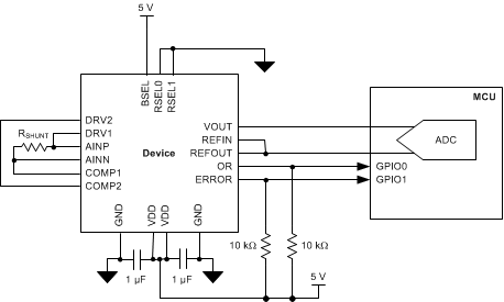 Figure 67. Simplified Schematic of a DRV425-Based Linear-Position Sensing Application
8.2.1.1 Design Requirements
For the example shown in Figure 67, use the parameters listed in Table 2 as a starting point of the design.
Table 2. Design Parameters
| DESIGN PARAMETER | EXAMPLE VALUE |
|---|---|
| Magnetic field range | VDD = 5 V: ±2 mT (max) VDD = 3.3 V: ±1.3 mT (max) |
| Supply voltage, VDD | 3.0 V to 5.5 V |
| Reference voltage, VREFIN | Range: GND to VDD If an internal reference is used: 2.5 V, 1.65 V, or VDD / 2 |
| Shunt resistor, RSHUNT | Depends on the desired magnetic field range, reference, and supply voltage; see the DRV425 System Parameter Calculator, SLOC331 for details. |
8.2.1.2 Detailed Design Procedure
Use the following procedure to design a solution for a linear-position sensor based on the DRV425:
- Select the proper supply voltage VDD to support the desired magnetic field range (see Table 2 for reference).
- Select the proper reference voltage VREFIN to support the desired magnetic field range and to match the input voltage specifications of the desired ADC.
- Use the DRV425 System Parameter Calculator, SLOC331 (RangeCalculator tab) to select the proper shunt resistor value of RSHUNT.
- The sensitivity drift performance of a DRV425-based linear position sensor is dominated by the temperature coefficient of the external shunt resistor. Select a low-drift shunt resistor for best sensor performance.
- Use the DRV425 System Parameter Calculator, SLOC331 (Problems Detected Table in DRV425 System Parameters tab) to verify the system response.
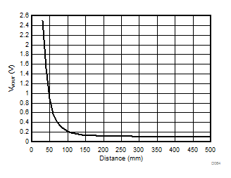
The amplitude of the magnetic field is a function of distance to and the shape of the magnet, as shown in Figure 69. If the magnetic field to be measured exceeds 3.6 mT, see the datasheet of the magnet to calculate the appropriate minimum distance to the DRV425 to avoid saturating the fluxgate sensor.
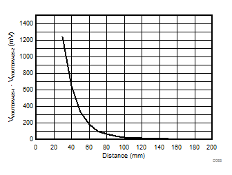
The high sensitivity of the DRV425 may require shielding of the sensing area to avoid influence of undesired magnetic field sources (such as the earth magnetic field). Alternatively, an additional DRV425 can be used to perform difference measurement to cancel the influence of a static magnetic field source, as shown in Figure 68. Figure 70 shows the differential voltage generated by two DRV425 devices in such a circuit.
 Figure 68. Differential Linear-Position Sensing Using Two DRV425 Devices
8.2.1.3 Application Curves
8.2.2 Current Sensing in Busbars
In existing applications that use busbars for power distribution, closed-loop current modules are usually used to accurately measure and control the current. These modules are usually bulky because of the required large magnetic core. Additionally, because the compensation current generated inside the module is proportional to the usually high busbar current, the power dissipation of this solution is usually as high as several watts.
Figure 71 shows an alternative approach with two DRV425 devices. If a hole is drilled in the middle of the busbar, the current is split in two equal parts that generate magnetic field gradients with opposite directions inside the hole. These magnetic fields are termed BR and BL in Figure 72. The opposite fields cancel each other out in the middle of the hole. The high sensitivity and linearity of two DRV425 devices positioned at the same distance from the middle of the hole allow the small opposite fields to be sensed and the current measured with high-accuracy levels. The differential measurement rejects outside fields that generate a common-mode error that is subtracted at the output.
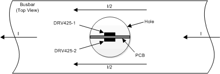 Figure 71. DRV425-Based Busbar Current Sensing
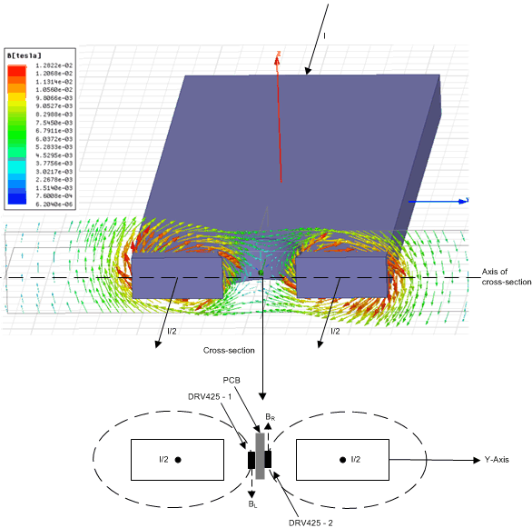 Figure 72. Magnetic Field Distribution Inside a Busbar Hole
8.2.2.1 Design Requirements
In order to measure the field gradient in the busbar, two DRV425 sensors are placed inside the hole at a well-defined distance by mounting them on opposite sides of a PCB that is inserted in the hole. The measurement range and resolution of this solution depends on the following factors:
- Busbar geometry: a wider busbar means a larger measurement range and lower resolution.
- Size of the hole: a larger diameter means a larger measurement range and lower resolution.
- Distance between the two DRV425 sensors: a smaller distance increases the measurement range and resolution.
Each of these factors can be optimized to create the desired measurement range for a particular application. Measurement ranges of ±250 A to ±1500 A are achievable with this approach. Larger currents are supported with large busbar structures and minimized distance between the two DRV425 sensors. Use the parameters listed in Table 3 as a starting point of the design.
Table 3. Design Parameters
| DESIGN PARAMETER | EXAMPLE VALUE | ||
|---|---|---|---|
| Current range | Up to ±1500 A | ||
| Supply voltage, VDD | 3.0 V to 5.5 V | ||
| Reference voltage, VREFIN | VDD / 2 | ||
8.2.2.2 Detailed Design Procedure
Figure 73 shows the schematic diagram of a differential gradient field measurement circuit.
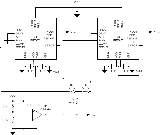 Figure 73. Schematic of a DRV425-Based Busbar Current-Sensing Circuit
In Figure 73, the feedback loops of both DRV425 sensors are combined to directly produce a differential output VDIFF that is proportional to the sensed magnetic field difference inside the busbar hole. Both compensation coils are connected in series and are driven from a single side of the compensation coil driver (the DRV1 pins of each DRV425). Therefore, both driver stages ensure that a current proportional to the magnetic fields BR and BL is driven through the respective compensation coil. The difference in current through both compensation coils, and thus the difference field between the sensors, flows through resistor R3 and is sensed by the shunt-sense amplifier of U2. The current proportional to the common-mode field inside the busbar hole flows through R1 and R2 and is sensed by the shunt-sense amplifier of U1.
Use the output VCM to verify that the sensors are correctly positioned in the busbar hole with the following steps:
- Measure VCM with no current flow through the busbar and the PCB in the middle of the busbar hole. This value is the offset voltage VOFFSET. The value of VOFFSET only depends on stray fields and varies little with the absolute position of the sensors.
- Apply current through the busbar and move the PCB along the y-axis in the busbar hole, as shown in Figure 72. The PCB is in the center of the hole if VCM = VOFFSET.
The sensitivity drift performance of the circuit shown in Figure 73 is dominated by the temperature coefficient of the external resistors R1, R2, and R3. Select low-drift resistors for best sensor performance. For overall system error calculation, also consider the affect of thermal expansion on the PCB and busbar.
The internal voltage reference of the DRV425 cannot be used in this application because of its limited driver capability. The OPA320 (U3) is a low-noise operational amplifier with a short-circuit current capability of ±65 mA and is used to support the required compensation current.
The advantage of this solution is its simplicity: the currents are subtracted by the two DRV425 devices without additional components. The series connection of the compensation coils halves the voltage swing and reduces the measurement range of the sensors also by 50%. If a larger sensing range is required, operate the two sensors independently and use a differential amplifier or ADC to subtract both voltage outputs (VOUT).
Use the ERROR outputs for fast overcurrent detection on the system level.
8.2.2.3 Application Curves
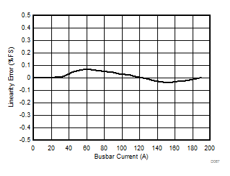
Figure 74 and Figure 75 show the measurement results on a 16-mm wide and 6-mm thick copper busbar with a 12-mm hole diameter using the circuit shown in Figure 73. The two DRV425 devices are placed at a distance of 1 mm from each other on opposite sides of the PCB. The measurement range is ±500 A; measurement results are limited by test setup. Independent operation of the two DRV425 sensors increases the measurement range to ±1000 A with the same busbar geometry.
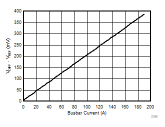
Busbar Current
