SBOS729A October 2015 – March 2016 DRV425
PRODUCTION DATA.
- 1 Features
- 2 Applications
- 3 Description
- 4 Revision History
- 5 Pin Configuration and Functions
- 6 Specifications
- 7 Detailed Description
- 8 Application and Implementation
- 9 Power-Supply Recommendations
- 10Layout
- 11Device and Documentation Support
- 12Mechanical, Packaging, and Orderable Information
10 Layout
10.1 Layout Guidelines
The unique, integrated fluxgate of the DRV425 has a very high sensitivity to enable designing a closed-loop magnetic-field sensor with best-in-class precision and linearity. Observe proper PCB layout techniques because any current-conducting wire in the direct vicinity of the DRV425 generates a magnetic field that can distort measurements. Common passive components and some PCB plating materials contain ferromagnetic materials that are magnetizable. For best performance, use the following layout guidelines:
- Route current-conducting wires in pairs: route a wire with an incoming supply current next to, or on top of, its return current path. The opposite magnetic field polarity of these connections cancel each other. To facilitate this layout approach, the DRV425 positive and negative supply pins are located next to each other.
- Route the compensation coil connections close to each other as a pair to reduce coupling effects.
- Minimize the length of the compensation coil connections between the DRV1/2 and COMP1/2 pins.
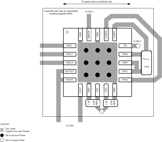
- Route currents parallel to the fluxgate sensor sensitivity axis as illustrated in Figure 76. As a result, magnetic fields are perpendicular to the fluxgate sensitivity and have limited affect.
- Vertical current flow (for example, through vias) generates a field in the fluxgate-sensitive direction. Minimize the number of vias in the vicinity of the DRV425.
- Use nonmagnetic passive components (for example, decoupling capacitors and the shunt resistor) to prevent magnetizing effects near the DRV425.
- Do not use PCB trace finishes with nickel-gold plating because of the potential for magnetization.
- Connect all GND pins to a local ground plane.
Ferrite beads in series to the power-supply connection reduce interaction with other circuits powered from the same supply voltage source. However, to prevent influence of the magnetic fields if ferrite beads are used, do not place them next to the DRV425.
The reference output (the REFOUT pin) refers to GND. Use a low-impedance and star-type connection to reduce the driver current and the fluxgate sensor current modulating the voltage drop on the ground track. The REFOUT and VOUT outputs are able to drive some capacitive load, but avoid large direct capacitive loading because of increased internal pulse currents. Given the wide bandwidth of the shunt-sense amplifier, isolate large capacitive loads with a small series resistor.
Solder the exposed PowerPAD on the bottom of the package to the ground layer because the PowerPAD is internally connected to the substrate that must be connected to the most-negative potential.
Figure 76 illustrates a generic layout example that highlights the placement of components that are critical to the DRV425 performance. For specific layout examples, see the DRV425EVM Users Guide, SLOU410.
10.2 Layout Example
 Figure 76. Generic Layout Example (Top View)