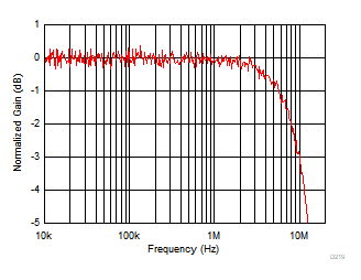
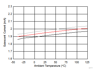
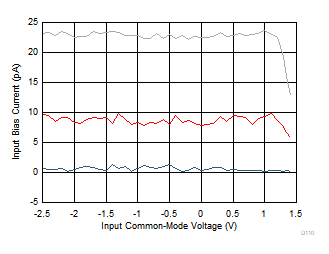
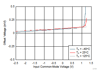
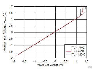
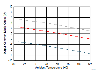
VS+ = 2.5 V, VS– = –2.5 V, VOCM = open, VICM = open, RF = 5 kΩ, G = 10 V/V, ICM loop disabled, RL = 1 kΩ, single-ended input, differential output, and input and output referenced to midsupply and TA ≈ 25°C, 1 (unless otherwise noted).
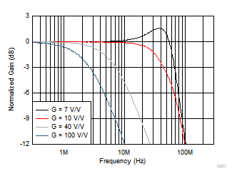 Figure 6-1 Small-Signal Frequency Response vs Gain
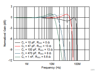 Figure 6-3 Small-Signal Frequency Response vs CL
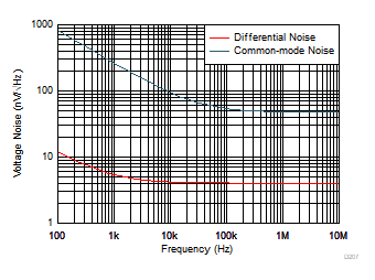 Figure 6-5 Input
Referred Voltage Noise vs Frequency
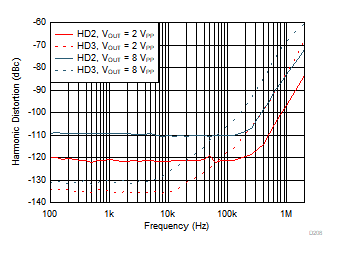 Figure 6-7 Harmonic Distortion vs Frequency
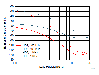 Figure 6-9 Harmonic Distortion vs RL
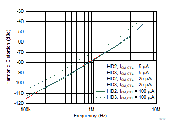
| VOUT = 8 VPP; Differential input to differential output; ICM Loop Enabled |
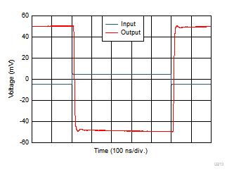 Figure 6-13 Small-Signal Transient Response
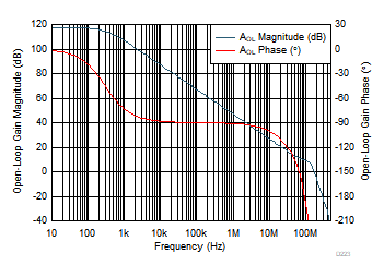 Figure 6-15 Open-Loop Gain
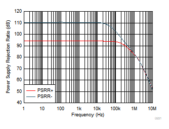 Figure 6-17 Power-Supply Rejection Ratio vs Frequency
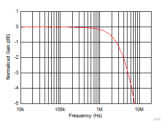
| VOCM
pin driven with 100 mVPP signal. Average
output voltage measured. |
Figure 6-19 VOCM
Loop Small-Signal Frequency Response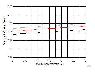 Figure 6-21 Quiescent Current vs Total Supply Voltage
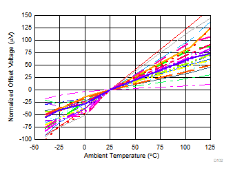 Figure 6-23 Offset Voltage vs Ambient Temperature
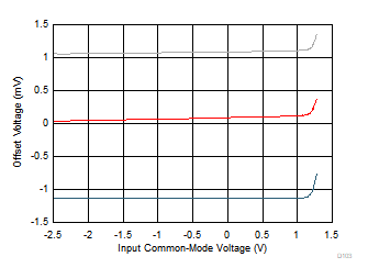 Figure 6-25 Offset Voltage vs Input Common-Mode Voltage
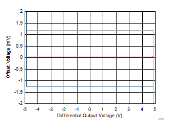
| 3
Typical Units, RL = 20 kΩ |
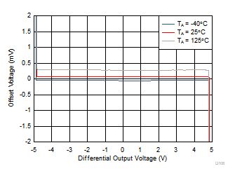
Figure 6-27 Offset Voltage vs Differential Output Voltage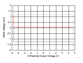
| 3
Typical Units, RL = 1 kΩ |
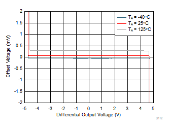
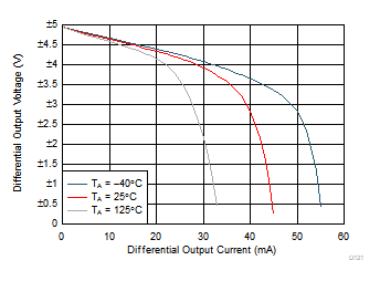
Figure 6-29 Offset Voltage vs Differential Output Voltage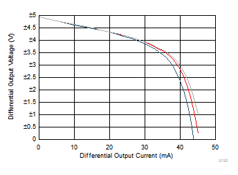 Figure 6-31 Differential Output Voltage vs Load Current
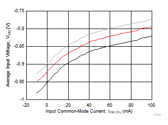
| VICM
pin floating, 3 Typical Units |
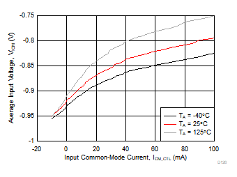
Figure 6-33 Average input Voltage vs Input Common-Mode Current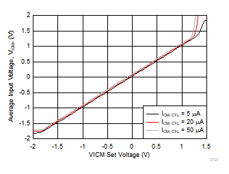 Figure 6-35 Average Input Voltage vs VICM Set Voltage
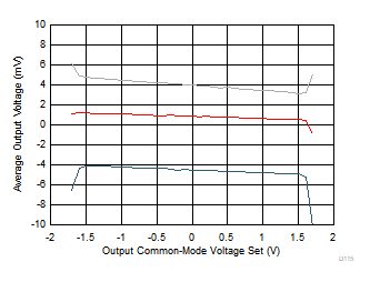
| VOCM
offset = (VOCM - VOCM), 3 Typical
Units |
Figure 6-37 Output Common-Mode Offset Voltage vs Output Common-Mode Set Voltage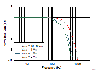 Figure 6-2 Frequency Response vs VOUT
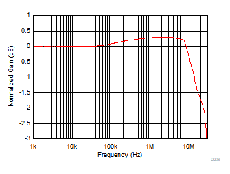 Figure 6-4 Large-Signal Frequency Response Flatness
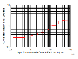
| f = 100 kHz, ICM loop enabled |
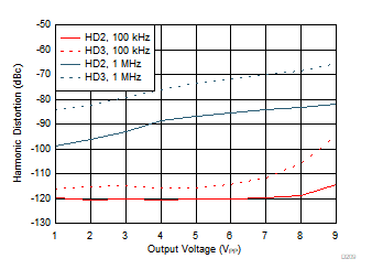 Figure 6-8 Harmonic Distortion vs VOUT
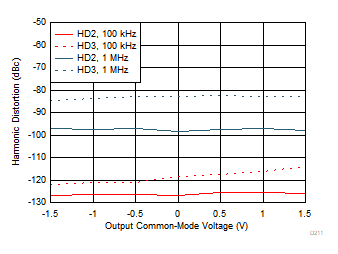 Figure 6-10 Harmonic Distortion vs VOCM
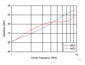
| VOUT = 2 VPP (each tone), Tone separation from center frequency = 100 kHz |
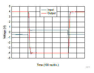
| Slew rate (rising and falling) = 500 V/µs |
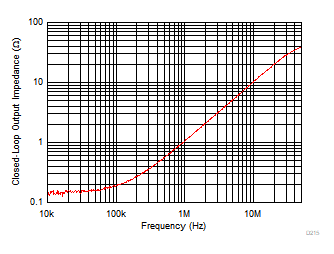
| G = 1 V/V, VOUT = 2 VPP, with VOCM adjusted |
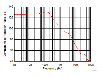 Figure 6-18 Common-Mode Rejection Ratio vs Frequency
| VICM
pin driven with 100 mVPP signal. Average
input voltage measured. |
Figure 6-20 VICM
Loop Small-Signal Frequency Response Figure 6-22 Quiescent Current vs Ambient Temperature
 Figure 6-24 Input
Bias Current vs Input Common-Mode Voltage
 Figure 6-26 Offset Voltage vs Input Common-Mode Voltage vs Ambient Temperature
 Figure 6-28 Offset Voltage vs Differential Output Voltage vs Ambient
Temperature
 Figure 6-30 Offset Voltage vs Differential Output Voltage vs Ambient
Temperature
 Figure 6-32 Differential Output Voltage vs Load Current vs Ambient Temperature
| VICM
pin floating, Typical Unit |
Figure 6-34 Average Input Voltage vs Input Common-Mode Current vs Ambient
Temperature
| ICM_CTL = 20 µA, Typical Unit |
Figure 6-36 Average Input Voltage vs VICM Set Voltage vs Ambient Temperature
| VOCM
= 0 V, 3 Typical Units |
Figure 6-38 Output Common-Mode Offset Voltage vs Ambient Temperature


 Figure 6-7 Harmonic Distortion vs Frequency


 Figure 6-17 Power-Supply Rejection Ratio vs Frequency


 Figure 6-8 Harmonic Distortion vs VOUT


 Figure 6-18 Common-Mode Rejection Ratio vs Frequency