SBOU246 January 2022 TMP61 , TMP61-Q1 , TMP63 , TMP63-Q1 , TMP64 , TMP64-Q1
2.2 Pinouts/Polarity
The TMP6 linear thermistor is a 2-pin device and therefore a pin-to-pin replacement of an NTC thermistor. These devices are also footprint-compatible as the TMP6 thermistor is offered in 0402 (1005-mm) and 0603 (1608-mm) packages. It should be noted that the 0603 part can also be used on an 0805 footprint. See Section 6.2 for more information.
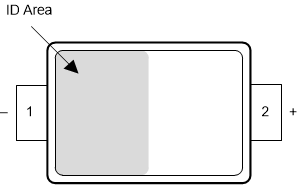
It is important to note that the TMP6 thermistor has polarity (see Figure 2-3).
 Figure 2-3 TMP6 Thermistor DYA Package 2-Pin SOT-5X3 Bottom View (Angled).
 TI uses a special silicon process where the doping level and active region areas devices control the key characteristics (the TCR and nominal resistance). The device has an active area and a substrate due to the polarized terminals. Connect the positive terminal to the highest voltage potential and the negative terminal to the lowest voltage potential to ensure proper operation. If the voltage across the pads is reversed, the thermistor will appear properly until the p-n junction starts to conduct (approximately 0.6 V), then the thermistor I-V characteristics will break down. This will result in a measurement of 0.6 V across the device terminals if configured reversely.