SBVS034O September   2003  – August 2025 TPS731

PRODUCTION DATA  

  1.   1
  2. Features
  3. Applications
  4. Description
  5. Pin Configuration and Functions
  6. Specifications
    1. 5.1 Absolute Maximum Ratings
    2. 5.2 ESD Ratings
    3. 5.3 Recommended Operating Conditions
    4. 5.4 Thermal Information
    5. 5.5 Electrical Characteristics
    6. 5.6 Typical Characteristics
  7. Detailed Description
    1. 6.1 Overview
    2. 6.2 Functional Block Diagrams
    3. 6.3 Feature Description
      1. 6.3.1 Output Noise
      2. 6.3.2 Internal Current Limit
      3. 6.3.3 Enable Pin and Shutdown
      4. 6.3.4 Reverse Current
    4. 6.4 Device Functional Modes
      1. 6.4.1 Normal Operation With 1.7 V ≤ VIN ≤ 5.5 V and VEN ≥ 1.7 V
  8. Application and Implementation
    1. 7.1 Application Information
    2. 7.2 Typical Application
      1. 7.2.1 Design Requirements
      2. 7.2.2 Detailed Design Procedure
        1. 7.2.2.1 Input and Output Capacitor Requirements
        2. 7.2.2.2 Dropout Voltage
        3. 7.2.2.3 Transient Response
      3. 7.2.3 Application Curves
    3. 7.3 Power Supply Recommendations
    4. 7.4 Layout
      1. 7.4.1 Layout Guidelines
        1. 7.4.1.1 Thermal Considerations
        2. 7.4.1.2 Power Dissipation
      2. 7.4.2 Layout Examples
  9. Device and Documentation Support
    1. 8.1 Device Support
      1. 8.1.1 Development Support
        1. 8.1.1.1 Spice Models
      2. 8.1.2 Device Nomenclature
    2. 8.2 Documentation Support
      1. 8.2.1 Related Documentation
    3. 8.3 Receiving Notification of Documentation Updates
    4. 8.4 Support Resources
    5. 8.5 Trademarks
    6. 8.6 Electrostatic Discharge Caution
    7. 8.7 Glossary
  10. Revision History
  11. 10Mechanical, Packaging, and Orderable Information

Pin Configuration and Functions

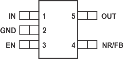
TPS731 DBV Package,5-Pin SOT-23,Top View Figure 4-1 DBV Package,5-Pin SOT-23,Top View
Table 4-1 Pin Functions
PIN I/O DESCRIPTION
NAME NO.
IN 1 I Input supply.
GND 2 Ground.
EN 3 I Driving the enable pin (EN) high turns on the regulator. Driving this pin low puts the regulator into shutdown mode. See the Enable Pin and Shutdown section for more details. EN can be connected to IN if not used.
NR 4 Fixed-voltage versions only—connecting an external capacitor to this pin bypasses noise generated by the internal bandgap, reducing output noise to very low levels.
FB 4 I Adjustable-voltage version only—this is the input to the control loop error amplifier, and is used to set the output voltage of the device.
OUT 5 O Output of the regulator. There are no output capacitor requirements for stability.